参数资料
| 型号: | XA3S1200E-4FTG256I |
| 厂商: | Xilinx Inc |
| 文件页数: | 20/37页 |
| 文件大小: | 0K |
| 描述: | IC FPGA SPARTAN3E 1200K 256FTBGA |
| 标准包装: | 90 |
| 系列: | Spartan®-3E XA |
| LAB/CLB数: | 8672 |
| 逻辑元件/单元数: | 19512 |
| RAM 位总计: | 516096 |
| 输入/输出数: | 190 |
| 门数: | 1200000 |
| 电源电压: | 1.14 V ~ 1.26 V |
| 安装类型: | 表面贴装 |
| 工作温度: | -40°C ~ 100°C |
| 封装/外壳: | 256-LBGA |
| 供应商设备封装: | 256-FTBGA |
第1页第2页第3页第4页第5页第6页第7页第8页第9页第10页第11页第12页第13页第14页第15页第16页第17页第18页第19页当前第20页第21页第22页第23页第24页第25页第26页第27页第28页第29页第30页第31页第32页第33页第34页第35页第36页第37页
DS635 (v2.0) September 9, 2009
Product Specification
27
R
Phase Shifter
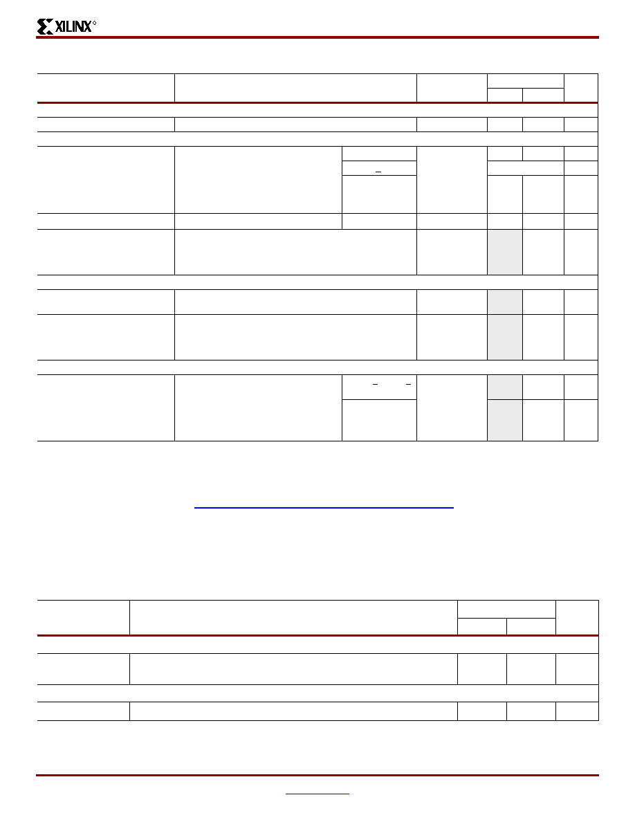
Table 29: Switching Characteristics for the DFS
Symbol
Description
Device
-4 Speed Grade
Units
Min
Max
Output Frequency Ranges
CLKOUT_FREQ_FX
Frequency for the CLKFX and CLKFX180 outputs
All
5
311
MHz
Output Clock Jitter(2,3)
CLKOUT_PER_JITT_FX
Period jitter at the CLKFX and CLKFX180
outputs
All
Typ
Max
CLKIN <20 MHz
See Note 4
ps
CLKIN > 20 MHz
±[1% of
CLKFX
period
+ 100]
±[1% of
CLKFX
period
+ 200]
ps
Duty Cycle(5,6)
CLKOUT_DUTY_CYCLE_FX
Duty cycle precision for the CLKFX and CLKFX180 outputs,
including the BUFGMUX and clock tree duty-cycle distortion
All
-±[1% of
CLKFX
period
+ 400]
ps
Phase Alignment(6)
CLKOUT_PHASE_FX
Phase offset between the DFS CLKFX output and the DLL CLK0
output when both the DFS and DLL are used
All
-
±200
ps
CLKOUT_PHASE_FX180
Phase offset between the DFS CLKFX180 output and the DLL
CLK0 output when both the DFS and DLL are used
All
-±[1% of
CLKFX
period
+ 300]
ps
Lock Time
LOCK_FX(2)
The time from deassertion at the DCM’s
Reset input to the rising transition at its
LOCKED output. The DFS asserts LOCKED
when the CLKFX and CLKFX180 signals
are valid. If using both the DLL and the DFS,
use the longer locking time.
5 MHz < FCLKIN <
15 MHz
All
-5
ms
FCLKIN > 15 MHz
-450
μs
Notes:
1.
2.
For optimal jitter tolerance and faster lock time, use the CLKIN_PERIOD attribute.
3.
Maximum output jitter is characterized within a reasonable noise environment (150 ps input period jitter, 40 SSOs and 25% CLB switching). Output
jitter strongly depends on the environment, including the number of SSOs, the output drive strength, CLB utilization, CLB switching activities, switching
frequency, power supply and PCB design. The actual maximum output jitter depends on the system application.
4.
Use the Spartan-3A Jitter Calculator (www.xilinx.com/support/documentation/data_sheets/s3a_jitter_calc.zip) to estimate DFS output jitter. Use the
Clocking Wizard to determine jitter for a specific design.
5.
The CLKFX and CLKFX180 outputs always have an approximate 50% duty cycle.
6.
Some duty-cycle and alignment specifications include 1% of the CLKFX output period or 0.01 UI. Example: The data sheet specifies a maximum jitter
of “±[1% of CLKFX period + 300]”. Assume the CLKFX output frequency is 100 MHz. The equivalent CLKFX period is 10 ns and 1% of 10 ns is 0.1 ns
or 100 ps. According to the data sheet, the maximum jitter is ±[100 ps + 300 ps] = ±400 ps.
Table 30: Recommended Operating Conditions for the PS in Variable Phase Mode
Symbol
Description
-4 Speed Grade
Units
Min
Max
Operating Frequency Ranges
PSCLK_FREQ
(FPSCLK)
Frequency for the PSCLK input
1
167
MHz
Input Pulse Requirements
PSCLK_PULSE
PSCLK pulse width as a percentage of the PSCLK period
40%
60%
-
相关PDF资料 |
PDF描述 |
|---|---|
| 93LC76A-E/ST | IC EEPROM 8KBIT 1024X8 8-TSSOP |
| 93LC76A-E/MS | IC EEPROM 8KBIT 1024X8 8-MSOP |
| 93C86BT-E/SN | IC EEPROM 16KBIT 1024X16 8-SOIC |
| XC2V80-5FGG256C | IC FPGA VIRTEX-II 80K 256-FBGA |
| 160-000-237R000 | DUST COVER FOR D-SUB37 FEMALE |
相关代理商/技术参数 |
参数描述 |
|---|---|
| XA3S1200E-4FTG256Q | 功能描述:IC FPGA SPARTAN3E 1200K 256FTBGA RoHS:是 类别:集成电路 (IC) >> 嵌入式 - FPGA(现场可编程门阵列) 系列:Spartan®-3E XA 标准包装:40 系列:Spartan® 6 LX LAB/CLB数:3411 逻辑元件/单元数:43661 RAM 位总计:2138112 输入/输出数:358 门数:- 电源电压:1.14 V ~ 1.26 V 安装类型:表面贴装 工作温度:-40°C ~ 100°C 封装/外壳:676-BGA 供应商设备封装:676-FBGA(27x27) |
| XA3S1400A | 制造商:XILINX 制造商全称:XILINX 功能描述:XA Spartan-3A Automotive FPGA Family Data Sheet |
| XA3S1400A-4FGG484I | 功能描述:IC FPGA SPARTAN3A 1400K 484-FBGA RoHS:是 类别:集成电路 (IC) >> 嵌入式 - FPGA(现场可编程门阵列) 系列:Spartan®-3A XA 产品变化通告:Step Intro and Pkg Change 11/March/2008 标准包装:1 系列:Virtex®-5 SXT LAB/CLB数:4080 逻辑元件/单元数:52224 RAM 位总计:4866048 输入/输出数:480 门数:- 电源电压:0.95 V ~ 1.05 V 安装类型:表面贴装 工作温度:-40°C ~ 100°C 封装/外壳:1136-BBGA,FCBGA 供应商设备封装:1136-FCBGA 配用:568-5088-ND - BOARD DEMO DAC1408D750122-1796-ND - EVALUATION PLATFORM VIRTEX-5 |
| XA3S1400A-4FGG484Q | 功能描述:IC FPGA SPARTAN3A 1400K 484-FBGA RoHS:是 类别:集成电路 (IC) >> 嵌入式 - FPGA(现场可编程门阵列) 系列:Spartan®-3A XA 产品变化通告:Step Intro and Pkg Change 11/March/2008 标准包装:1 系列:Virtex®-5 SXT LAB/CLB数:4080 逻辑元件/单元数:52224 RAM 位总计:4866048 输入/输出数:480 门数:- 电源电压:0.95 V ~ 1.05 V 安装类型:表面贴装 工作温度:-40°C ~ 100°C 封装/外壳:1136-BBGA,FCBGA 供应商设备封装:1136-FCBGA 配用:568-5088-ND - BOARD DEMO DAC1408D750122-1796-ND - EVALUATION PLATFORM VIRTEX-5 |
| XA3S1500-4FGG456I | 功能描述:IC FPGA SPARTAN-3 1.5M 456-FBGA RoHS:是 类别:集成电路 (IC) >> 嵌入式 - FPGA(现场可编程门阵列) 系列:Spartan®-3 XA 产品变化通告:Step Intro and Pkg Change 11/March/2008 标准包装:1 系列:Virtex®-5 SXT LAB/CLB数:4080 逻辑元件/单元数:52224 RAM 位总计:4866048 输入/输出数:480 门数:- 电源电压:0.95 V ~ 1.05 V 安装类型:表面贴装 工作温度:-40°C ~ 100°C 封装/外壳:1136-BBGA,FCBGA 供应商设备封装:1136-FCBGA 配用:568-5088-ND - BOARD DEMO DAC1408D750122-1796-ND - EVALUATION PLATFORM VIRTEX-5 |
发布紧急采购,3分钟左右您将得到回复。