- 您现在的位置:买卖IC网 > PDF目录277726 > XA3S250E-4TQG144I (XILINX INC) FPGA, 612 CLBS, 250000 GATES, 572 MHz, PQFP144 PDF资料下载
参数资料
| 型号: | XA3S250E-4TQG144I |
| 厂商: | XILINX INC |
| 元件分类: | FPGA |
| 英文描述: | FPGA, 612 CLBS, 250000 GATES, 572 MHz, PQFP144 |
| 封装: | LEAD FREE, TQFP-144 |
| 文件页数: | 26/37页 |
| 文件大小: | 717K |
| 代理商: | XA3S250E-4TQG144I |
第1页第2页第3页第4页第5页第6页第7页第8页第9页第10页第11页第12页第13页第14页第15页第16页第17页第18页第19页第20页第21页第22页第23页第24页第25页当前第26页第27页第28页第29页第30页第31页第32页第33页第34页第35页第36页第37页
DS635 (v2.0) September 9, 2009
Product Specification
32
R
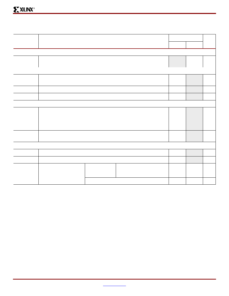
Slave Parallel Mode Timing
Table 39: Timing for the Slave Parallel Configuration Mode
Symbol
Description
-4 Speed Grade
Units
Min
Max
Clock-to-Output Times
TSMCKBY
The time from the rising transition on the CCLK pin to a signal transition at the
BUSY pin
-12.0
ns
Setup Times
TSMDCC
The time from the setup of data at the D0-D7 pins to the active edge the CCLK
pin
11.0
-ns
TSMCSCC
Setup time on the CSI_B pin before the active edge of the CCLK pin
10.0
-ns
TSMCCW(2)
Setup time on the RDWR_B pin before active edge of the CCLK pin
23.0
-ns
Hold Times
TSMCCD
The time from the active edge of the CCLK pin to the point when data is last
held at the D0-D7 pins
1.0
-ns
TSMCCCS
The time from the active edge of the CCLK pin to the point when a logic level
is last held at the CSO_B pin
0
-ns
TSMWCC
The time from the active edge of the CCLK pin to the point when a logic level
is last held at the RDWR_B pin
0
-ns
Clock Timing
TCCH
The High pulse width at the CCLK input pin
5
-ns
TCCL
The Low pulse width at the CCLK input pin
5
-ns
FCCPAR
Frequency of the clock
signal at the CCLK input
pin
No bitstream
compression
Not using the BUSY pin(2)
050
MHz
Using the BUSY pin
0
66
MHz
With bitstream compression
0
20
MHz
Notes:
1.
The numbers in this table are based on the operating conditions set forth in Table 6.
2.
In the Slave Parallel mode, it is necessary to use the BUSY pin when the CCLK frequency exceeds this maximum specification.
3.
Some Xilinx documents refer to Parallel modes as “SelectMAP” modes.
相关PDF资料 |
PDF描述 |
|---|---|
| XD-14596F4-364W | SYNCHRO OR RESOLVER TO DIGITAL CONVERTER, CDFP36 |
| XD-14596F4-372Q | SYNCHRO OR RESOLVER TO DIGITAL CONVERTER, CDFP36 |
| XD-14596F4-432 | SYNCHRO OR RESOLVER TO DIGITAL CONVERTER, CDFP36 |
| XD-14596F4-462L | SYNCHRO OR RESOLVER TO DIGITAL CONVERTER, CDFP36 |
| XD-14596F4-504W | SYNCHRO OR RESOLVER TO DIGITAL CONVERTER, CDFP36 |
相关代理商/技术参数 |
参数描述 |
|---|---|
| XA3S250E-4TQG144Q | 功能描述:IC FPGA SPARTAN-3E 250K 144-TQFP RoHS:是 类别:集成电路 (IC) >> 嵌入式 - FPGA(现场可编程门阵列) 系列:Spartan®-3E XA 标准包装:40 系列:Spartan® 6 LX LAB/CLB数:3411 逻辑元件/单元数:43661 RAM 位总计:2138112 输入/输出数:358 门数:- 电源电压:1.14 V ~ 1.26 V 安装类型:表面贴装 工作温度:-40°C ~ 100°C 封装/外壳:676-BGA 供应商设备封装:676-FBGA(27x27) |
| XA3S250E-4VQG100I | 功能描述:IC FPGA SPARTAN-3E 250K 100-VQFP RoHS:是 类别:集成电路 (IC) >> 嵌入式 - FPGA(现场可编程门阵列) 系列:Spartan®-3E XA 标准包装:40 系列:Spartan® 6 LX LAB/CLB数:3411 逻辑元件/单元数:43661 RAM 位总计:2138112 输入/输出数:358 门数:- 电源电压:1.14 V ~ 1.26 V 安装类型:表面贴装 工作温度:-40°C ~ 100°C 封装/外壳:676-BGA 供应商设备封装:676-FBGA(27x27) |
| XA3S250E-4VQG100Q | 功能描述:IC FPGA SPARTAN-3E 250K 100-VQFP RoHS:是 类别:集成电路 (IC) >> 嵌入式 - FPGA(现场可编程门阵列) 系列:Spartan®-3E XA 标准包装:40 系列:Spartan® 6 LX LAB/CLB数:3411 逻辑元件/单元数:43661 RAM 位总计:2138112 输入/输出数:358 门数:- 电源电压:1.14 V ~ 1.26 V 安装类型:表面贴装 工作温度:-40°C ~ 100°C 封装/外壳:676-BGA 供应商设备封装:676-FBGA(27x27) |
| XA3S400-4FGG456I | 功能描述:IC FPGA SPARTAN-3 400K 456-FBGA RoHS:是 类别:集成电路 (IC) >> 嵌入式 - FPGA(现场可编程门阵列) 系列:Spartan®-3 XA 标准包装:40 系列:Spartan® 6 LX LAB/CLB数:3411 逻辑元件/单元数:43661 RAM 位总计:2138112 输入/输出数:358 门数:- 电源电压:1.14 V ~ 1.26 V 安装类型:表面贴装 工作温度:-40°C ~ 100°C 封装/外壳:676-BGA 供应商设备封装:676-FBGA(27x27) |
| XA3S400-4FGG456Q | 功能描述:IC FPGA SPARTAN-3 400K 456-FBGA RoHS:是 类别:集成电路 (IC) >> 嵌入式 - FPGA(现场可编程门阵列) 系列:Spartan®-3 XA 标准包装:40 系列:Spartan® 6 LX LAB/CLB数:3411 逻辑元件/单元数:43661 RAM 位总计:2138112 输入/输出数:358 门数:- 电源电压:1.14 V ~ 1.26 V 安装类型:表面贴装 工作温度:-40°C ~ 100°C 封装/外壳:676-BGA 供应商设备封装:676-FBGA(27x27) |
发布紧急采购,3分钟左右您将得到回复。