- 您现在的位置:买卖IC网 > PDF目录277726 > XA3S250E-4TQG144I (XILINX INC) FPGA, 612 CLBS, 250000 GATES, 572 MHz, PQFP144 PDF资料下载
参数资料
| 型号: | XA3S250E-4TQG144I |
| 厂商: | XILINX INC |
| 元件分类: | FPGA |
| 英文描述: | FPGA, 612 CLBS, 250000 GATES, 572 MHz, PQFP144 |
| 封装: | LEAD FREE, TQFP-144 |
| 文件页数: | 8/37页 |
| 文件大小: | 717K |
| 代理商: | XA3S250E-4TQG144I |
第1页第2页第3页第4页第5页第6页第7页当前第8页第9页第10页第11页第12页第13页第14页第15页第16页第17页第18页第19页第20页第21页第22页第23页第24页第25页第26页第27页第28页第29页第30页第31页第32页第33页第34页第35页第36页第37页
DS635 (v2.0) September 9, 2009
Product Specification
16
R
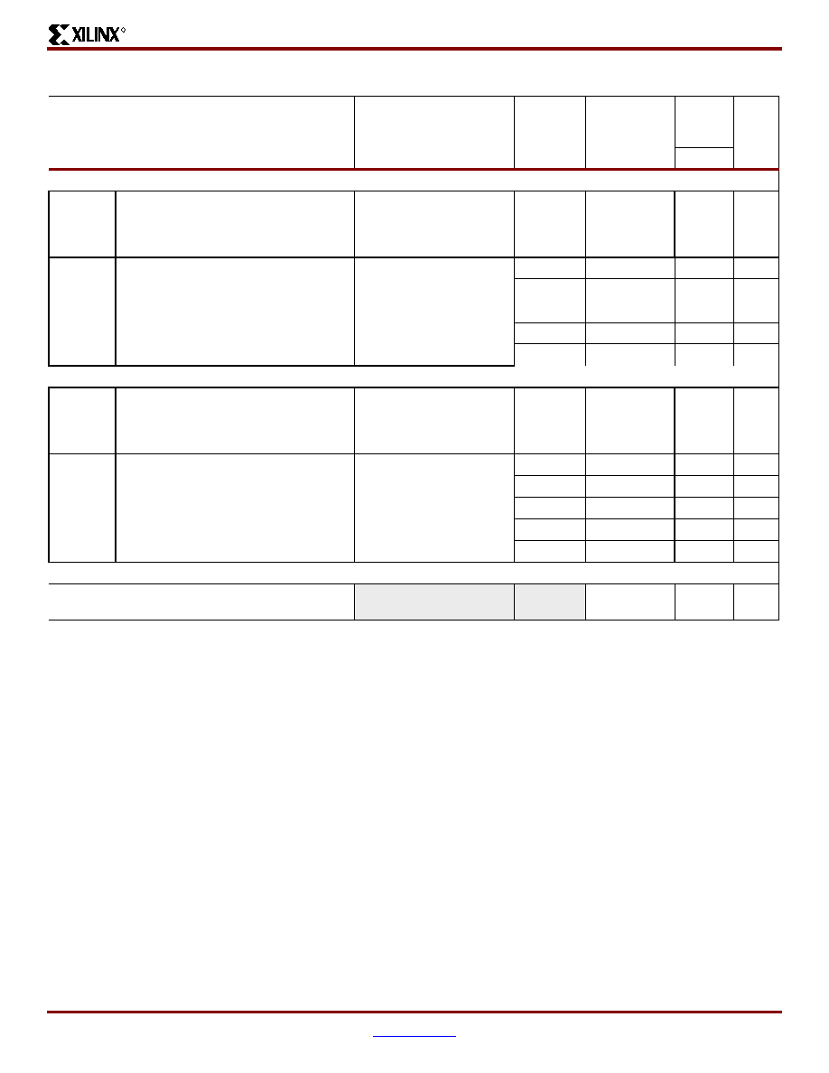
Table 15: Setup and Hold Times for the IOB Input Path
Symbol
Description
Conditions
IFD_
DELAY_
VALUE
Device
-4
Speed
Grade
Units
Min
Setup Times
TIOPICK
Time from the setup of data at the Input
pin to the active transition at the ICLK input
of the Input Flip-Flop (IFF). No Input Delay
is programmed.
LVCMOS25(2),
IFD_DELAY_VALUE = 0
0All
2.12
ns
TIOPICKD
Time from the setup of data at the Input
pin to the active transition at the IFF’s ICLK
input. The Input Delay is programmed.
LVCMOS25(2),
IFD_DELAY_VALUE =
default software setting
2
XA3S100E
6.49
ns
3
XA3S250E
6.85
ns
2
XA3S500E
7.01
ns
5
XA3S1200E
8.67
ns
4
XA3S1600E
7.69
ns
Hold Times
TIOICKP
Time from the active transition at the IFF’s
ICLK input to the point where data must be
held at the Input pin. No Input Delay is
programmed.
LVCMOS25(2),
IFD_DELAY_VALUE = 0
0All
–0.76
ns
TIOICKPD
Time from the active transition at the IFF’s
ICLK input to the point where data must be
held at the Input pin. The Input Delay is
programmed.
LVCMOS25(2),
IFD_DELAY_VALUE =
default software setting
2
XA3S100E
–3.93
ns
3
XA3S250E
–3.51
ns
2
XA3S500E
–3.74
ns
5
XA3S1200E
–4.30
ns
4
XA3S1600E
–4.14
ns
Set/Reset Pulse Width
TRPW_IOB
Minimum pulse width to SR control input
on IOB
All
1.80
ns
Notes:
1.
The numbers in this table are tested using the methodology presented in Table 19 and are based on the operating conditions set forth in
2.
This setup time requires adjustment whenever a signal standard other than LVCMOS25 is assigned to the data Input. If this is true, add the
appropriate Input adjustment from Table 17.
3.
These hold times require adjustment whenever a signal standard other than LVCMOS25 is assigned to the data Input. If this is true, subtract
the appropriate Input adjustment from Table 17. When the hold time is negative, it is possible to change the data before the clock’s active
edge.
相关PDF资料 |
PDF描述 |
|---|---|
| XD-14596F4-364W | SYNCHRO OR RESOLVER TO DIGITAL CONVERTER, CDFP36 |
| XD-14596F4-372Q | SYNCHRO OR RESOLVER TO DIGITAL CONVERTER, CDFP36 |
| XD-14596F4-432 | SYNCHRO OR RESOLVER TO DIGITAL CONVERTER, CDFP36 |
| XD-14596F4-462L | SYNCHRO OR RESOLVER TO DIGITAL CONVERTER, CDFP36 |
| XD-14596F4-504W | SYNCHRO OR RESOLVER TO DIGITAL CONVERTER, CDFP36 |
相关代理商/技术参数 |
参数描述 |
|---|---|
| XA3S250E-4TQG144Q | 功能描述:IC FPGA SPARTAN-3E 250K 144-TQFP RoHS:是 类别:集成电路 (IC) >> 嵌入式 - FPGA(现场可编程门阵列) 系列:Spartan®-3E XA 标准包装:40 系列:Spartan® 6 LX LAB/CLB数:3411 逻辑元件/单元数:43661 RAM 位总计:2138112 输入/输出数:358 门数:- 电源电压:1.14 V ~ 1.26 V 安装类型:表面贴装 工作温度:-40°C ~ 100°C 封装/外壳:676-BGA 供应商设备封装:676-FBGA(27x27) |
| XA3S250E-4VQG100I | 功能描述:IC FPGA SPARTAN-3E 250K 100-VQFP RoHS:是 类别:集成电路 (IC) >> 嵌入式 - FPGA(现场可编程门阵列) 系列:Spartan®-3E XA 标准包装:40 系列:Spartan® 6 LX LAB/CLB数:3411 逻辑元件/单元数:43661 RAM 位总计:2138112 输入/输出数:358 门数:- 电源电压:1.14 V ~ 1.26 V 安装类型:表面贴装 工作温度:-40°C ~ 100°C 封装/外壳:676-BGA 供应商设备封装:676-FBGA(27x27) |
| XA3S250E-4VQG100Q | 功能描述:IC FPGA SPARTAN-3E 250K 100-VQFP RoHS:是 类别:集成电路 (IC) >> 嵌入式 - FPGA(现场可编程门阵列) 系列:Spartan®-3E XA 标准包装:40 系列:Spartan® 6 LX LAB/CLB数:3411 逻辑元件/单元数:43661 RAM 位总计:2138112 输入/输出数:358 门数:- 电源电压:1.14 V ~ 1.26 V 安装类型:表面贴装 工作温度:-40°C ~ 100°C 封装/外壳:676-BGA 供应商设备封装:676-FBGA(27x27) |
| XA3S400-4FGG456I | 功能描述:IC FPGA SPARTAN-3 400K 456-FBGA RoHS:是 类别:集成电路 (IC) >> 嵌入式 - FPGA(现场可编程门阵列) 系列:Spartan®-3 XA 标准包装:40 系列:Spartan® 6 LX LAB/CLB数:3411 逻辑元件/单元数:43661 RAM 位总计:2138112 输入/输出数:358 门数:- 电源电压:1.14 V ~ 1.26 V 安装类型:表面贴装 工作温度:-40°C ~ 100°C 封装/外壳:676-BGA 供应商设备封装:676-FBGA(27x27) |
| XA3S400-4FGG456Q | 功能描述:IC FPGA SPARTAN-3 400K 456-FBGA RoHS:是 类别:集成电路 (IC) >> 嵌入式 - FPGA(现场可编程门阵列) 系列:Spartan®-3 XA 标准包装:40 系列:Spartan® 6 LX LAB/CLB数:3411 逻辑元件/单元数:43661 RAM 位总计:2138112 输入/输出数:358 门数:- 电源电压:1.14 V ~ 1.26 V 安装类型:表面贴装 工作温度:-40°C ~ 100°C 封装/外壳:676-BGA 供应商设备封装:676-FBGA(27x27) |
发布紧急采购,3分钟左右您将得到回复。