参数资料
| 型号: | XA3SD3400A-4FGG676I |
| 厂商: | Xilinx Inc |
| 文件页数: | 22/58页 |
| 文件大小: | 0K |
| 描述: | SPARTAN-3ADSP FPGA 3400K 676FBGA |
| 产品培训模块: | Extended Spartan 3A FPGA Family |
| 标准包装: | 40 |
| 系列: | Spartan®-3A DSP XA |
| LAB/CLB数: | 5968 |
| 逻辑元件/单元数: | 53712 |
| RAM 位总计: | 2322432 |
| 输入/输出数: | 469 |
| 门数: | 3400000 |
| 电源电压: | 1.14 V ~ 1.26 V |
| 安装类型: | 表面贴装 |
| 工作温度: | -40°C ~ 100°C |
| 封装/外壳: | 676-BGA |
| 供应商设备封装: | 676-FBGA(27x27) |
第1页第2页第3页第4页第5页第6页第7页第8页第9页第10页第11页第12页第13页第14页第15页第16页第17页第18页第19页第20页第21页当前第22页第23页第24页第25页第26页第27页第28页第29页第30页第31页第32页第33页第34页第35页第36页第37页第38页第39页第40页第41页第42页第43页第44页第45页第46页第47页第48页第49页第50页第51页第52页第53页第54页第55页第56页第57页第58页
XA Spartan-3A DSP Automotive FPGA Family Data Sheet
DS705 (v2.0) April 18, 2011
Product Specification
29
Timing Measurement Methodology
When measuring timing parameters at the programmable I/Os, different signal standards call for different test conditions.
Table 27 lists the conditions to use for each standard.
The method for measuring Input timing is as follows: A signal that swings between a Low logic level of VL and a High logic
level of VH is applied to the Input under test. Some standards also require the application of a bias voltage to the VREF pins
of a given bank to properly set the input-switching threshold. The measurement point of the Input signal (VM) is commonly
located halfway between VL and VH.
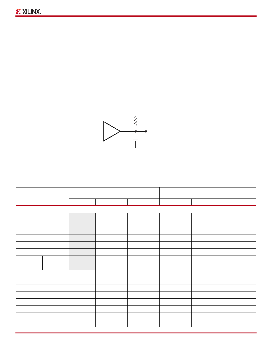
The Output test setup is shown in Figure 9. A termination voltage VT is applied to the termination resistor RT, the other end
of which is connected to the Output. For each standard, RT and VT generally take on the standard values recommended for
minimizing signal reflections. If the standard does not ordinarily use terminations (for example, LVCMOS, LVTTL), then RT
is set to 1 M
to indicate an open connection, and V
T is set to zero. The same measurement point (VM) that was used at the
Input is also used at the Output.
X-Ref Target - Figure 9
Figure 9: Output Test Setup
Table 27: Test Methods for Timing Measurement at I/Os
Signal Standard
(IOSTANDARD)
Inputs
Outputs
Inputs and
Outputs
VREF (V)
VL (V)
VH (V)
RT ()VT (V)
VM (V)
Single-Ended
LVTTL
–
0
3.3
1M
0
1.4
LVCMOS33
–
0
3.3
1M
0
1.65
LVCMOS25
–
0
2.5
1M
0
1.25
LVCMOS18
–
0
1.8
1M
0
0.9
LVCMOS15
–
0
1.5
1M
0
0.75
LVCMOS12
–
0
1.2
1M
0
0.6
PCI33_3
Rising
–Note 3
Note 3
25
0
0.94
Falling
25
3.3
2.03
HSTL_I
0.75
VREF – 0.5
VREF + 0.5
50
0.75
VREF
HSTL_III
0.9
VREF – 0.5
VREF + 0.5
50
1.5
VREF
HSTL_I_18
0.9
VREF – 0.5
VREF + 0.5
50
0.9
VREF
HSTL_II_18
0.9
VREF – 0.5
VREF + 0.5
25
0.9
VREF
HSTL_III_18
1.1
VREF – 0.5
VREF + 0.5
50
1.8
VREF
SSTL18_I
0.9
VREF – 0.5
VREF + 0.5
50
0.9
VREF
SSTL18_II
0.9
VREF – 0.5
VREF + 0.5
25
0.9
VREF
SSTL2_I
1.25
VREF – 0.75
VREF + 0.75
50
1.25
VREF
FPGA Output
VT (VREF)
RT (RREF)
VM (VMEAS)
CL (CREF)
DS705_09_041311
Notes:
1.
The names shown in parentheses are
used in the IBIS file.
相关PDF资料 |
PDF描述 |
|---|---|
| XA6SLX75T-3FGG484Q | IC FPGA SPARTAN 6 484FGGBGA |
| XA95144XL-15CSG144I | IC CPLD 144MC 117 I/O 144CSBGA |
| XAM1808AZCE4 | IC ARM PROCESSOR 361NFBGA |
| XC1765ESOG8C | IC PROM SERIAL 65K 8-SOIC |
| XC17S200AVQ44I | IC PROM SER 200000 I-TEMP 44VQFP |
相关代理商/技术参数 |
参数描述 |
|---|---|
| X-A4A-300L | 制造商:Leach International Corporation 功能描述:MID RANGE - Bulk |
| X-A4C-300M | 制造商:Leach International Corporation 功能描述:MID RANGE - Bulk |
| X-A4M-300L | 制造商:Leach International Corporation 功能描述:MID RANGE - Bulk |
| X-A4M-300M | 制造商:Leach International Corporation 功能描述:MID RANGE - Bulk |
| X-A4N | 制造商:Leach International Corporation 功能描述:MID RANGE - Bulk |
发布紧急采购,3分钟左右您将得到回复。