参数资料
| 型号: | XA3SD3400A-4FGG676I |
| 厂商: | Xilinx Inc |
| 文件页数: | 5/58页 |
| 文件大小: | 0K |
| 描述: | SPARTAN-3ADSP FPGA 3400K 676FBGA |
| 产品培训模块: | Extended Spartan 3A FPGA Family |
| 标准包装: | 40 |
| 系列: | Spartan®-3A DSP XA |
| LAB/CLB数: | 5968 |
| 逻辑元件/单元数: | 53712 |
| RAM 位总计: | 2322432 |
| 输入/输出数: | 469 |
| 门数: | 3400000 |
| 电源电压: | 1.14 V ~ 1.26 V |
| 安装类型: | 表面贴装 |
| 工作温度: | -40°C ~ 100°C |
| 封装/外壳: | 676-BGA |
| 供应商设备封装: | 676-FBGA(27x27) |
第1页第2页第3页第4页当前第5页第6页第7页第8页第9页第10页第11页第12页第13页第14页第15页第16页第17页第18页第19页第20页第21页第22页第23页第24页第25页第26页第27页第28页第29页第30页第31页第32页第33页第34页第35页第36页第37页第38页第39页第40页第41页第42页第43页第44页第45页第46页第47页第48页第49页第50页第51页第52页第53页第54页第55页第56页第57页第58页
XA Spartan-3A DSP Automotive FPGA Family Data Sheet
DS705 (v2.0) April 18, 2011
Product Specification
13
Differential I/O Standards
HSTL_I(4)
8–8
0.4
VCCO – 0.4
24(7)
–8
0.4
VCCO – 0.4
HSTL_I_18
8
–8
0.4
VCCO – 0.4
16
–16(7)
0.4
VCCO – 0.4
HSTL_III_18
24(7)
–8
0.4
VCCO – 0.4
SSTL18_I
6.7
–6.7
VTT – 0.475
VTT + 0.475
SSTL18_II(4)
13.4
–13.4
VTT – 0.475
VTT + 0.475
SSTL2_I
8.1
–8.1
VTT – 0.61
VTT + 0.61
16.2
–16.2
VTT – 0.80
VTT + 0.80
SSTL3_I
8
–8
VTT – 0.6
VTT + 0.6
SSTL3_II
16
–16
VTT – 0.8
VTT + 0.8
Notes:
1.
2.
Descriptions of the symbols used in this table are as follows:
IOL – the output current condition under which VOL is tested
IOH – the output current condition under which VOH is tested
VOL – the output voltage that indicates a Low logic level
VOH – the output voltage that indicates a High logic level
VIL – the input voltage that indicates a Low logic level
VIH – the input voltage that indicates a High logic level
VCCO – the supply voltage for output drivers
VREF – the reference voltage for setting the input switching threshold
VTT – the voltage applied to a resistor termination
3.
For the LVCMOS and LVTTL standards: the same VOL and VOH limits apply for both the Fast and Slow slew attributes.
4.
These higher-drive output standards are supported only on FPGA banks 1 and 3. Inputs are unrestricted. See the chapter "Using I/O
Resources" in UG331.
5.
Tested according to the relevant PCI specifications. For information on PCI IP solutions, see
http://www.xilinx.com/products/design_resources/conn_central/protocols/pci_pcix.htm. The PCI IOSTANDARD is not supported on
input-only pins. The PCIX IOSTANDARD is available and has equivalent characteristics, but no PCI-X IP is supported.
6.
Derate by 20% for TJ above 100oC
7.
Derate by 5% for TJ above 100oC
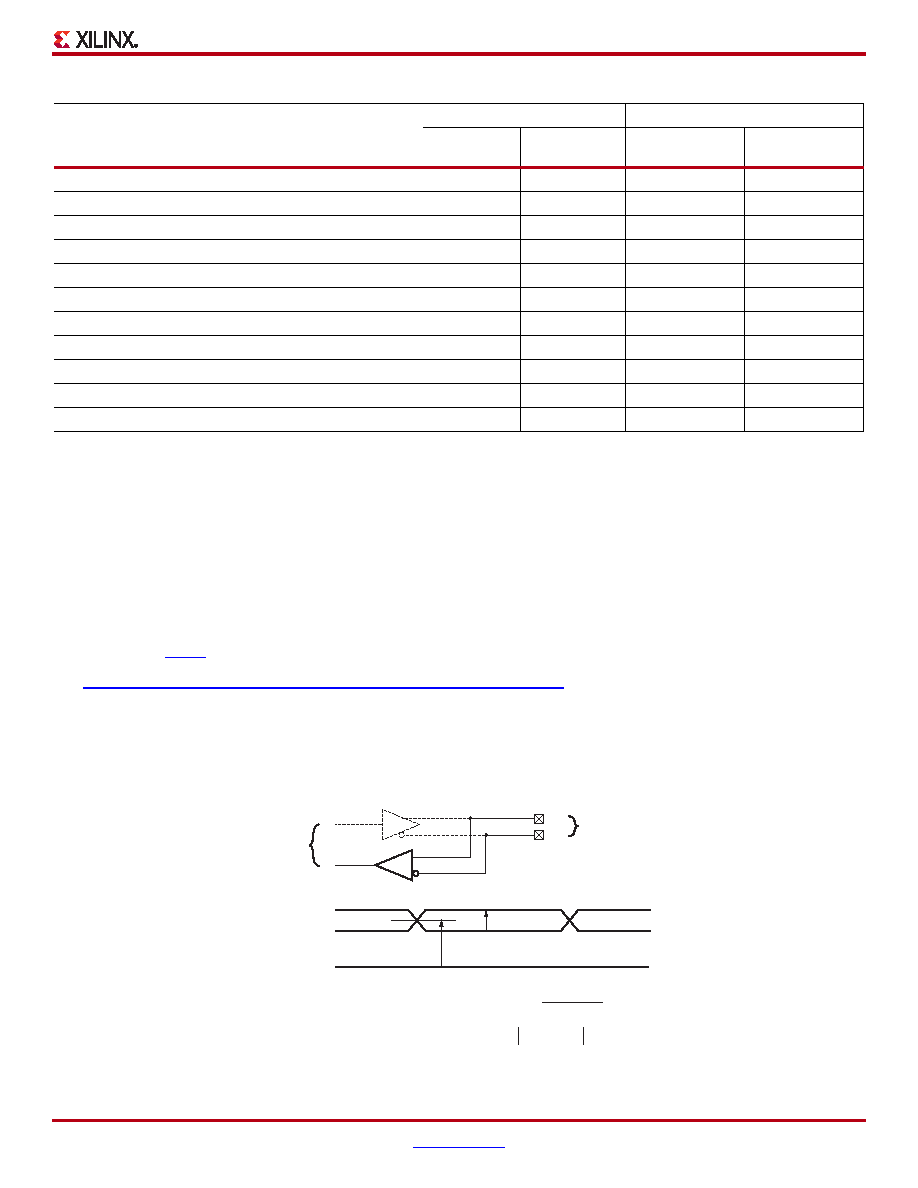
X-Ref Target - Figure 4
Figure 4: Differential Input Voltages
Table 12: DC Characteristics of User I/Os Using Single-Ended Standards (Cont’d)
IOSTANDARD Attribute
Test Conditions
Logic Level Characteristics
IOL
(mA)
IOH
(mA)
VOL
Max (V)
VOH
Min (V)
DS705_04_041111
V
INN
V
INN
V
INP
V
INP
GND level
50%
V
ICM
V
ICM = Input common mode voltage =
V
ID
Internal
Logic
Differential
I/O Pair Pins
N
P
2
V
INP
+ V
INN
V
ID = Differential input voltage =
V
INP
- V
INN
相关PDF资料 |
PDF描述 |
|---|---|
| XA6SLX75T-3FGG484Q | IC FPGA SPARTAN 6 484FGGBGA |
| XA95144XL-15CSG144I | IC CPLD 144MC 117 I/O 144CSBGA |
| XAM1808AZCE4 | IC ARM PROCESSOR 361NFBGA |
| XC1765ESOG8C | IC PROM SERIAL 65K 8-SOIC |
| XC17S200AVQ44I | IC PROM SER 200000 I-TEMP 44VQFP |
相关代理商/技术参数 |
参数描述 |
|---|---|
| X-A4A-300L | 制造商:Leach International Corporation 功能描述:MID RANGE - Bulk |
| X-A4C-300M | 制造商:Leach International Corporation 功能描述:MID RANGE - Bulk |
| X-A4M-300L | 制造商:Leach International Corporation 功能描述:MID RANGE - Bulk |
| X-A4M-300M | 制造商:Leach International Corporation 功能描述:MID RANGE - Bulk |
| X-A4N | 制造商:Leach International Corporation 功能描述:MID RANGE - Bulk |
发布紧急采购,3分钟左右您将得到回复。