参数资料
| 型号: | XC2S150-5FG256C |
| 厂商: | Xilinx Inc |
| 文件页数: | 51/99页 |
| 文件大小: | 0K |
| 描述: | IC FPGA 2.5V 864 CLB'S 256-FBGA |
| 标准包装: | 90 |
| 系列: | Spartan®-II |
| LAB/CLB数: | 864 |
| 逻辑元件/单元数: | 3888 |
| RAM 位总计: | 49152 |
| 输入/输出数: | 176 |
| 门数: | 150000 |
| 电源电压: | 2.375 V ~ 2.625 V |
| 安装类型: | 表面贴装 |
| 工作温度: | 0°C ~ 85°C |
| 封装/外壳: | 256-BGA |
| 供应商设备封装: | 256-FBGA(17x17) |
| 其它名称: | 122-1230 XC2S150-5FG256C-ND |
第1页第2页第3页第4页第5页第6页第7页第8页第9页第10页第11页第12页第13页第14页第15页第16页第17页第18页第19页第20页第21页第22页第23页第24页第25页第26页第27页第28页第29页第30页第31页第32页第33页第34页第35页第36页第37页第38页第39页第40页第41页第42页第43页第44页第45页第46页第47页第48页第49页第50页当前第51页第52页第53页第54页第55页第56页第57页第58页第59页第60页第61页第62页第63页第64页第65页第66页第67页第68页第69页第70页第71页第72页第73页第74页第75页第76页第77页第78页第79页第80页第81页第82页第83页第84页第85页第86页第87页第88页第89页第90页第91页第92页第93页第94页第95页第96页第97页第98页第99页
Spartan-II FPGA Family: DC and Switching Characteristics
DS001-3 (v2.8) June 13, 2008
Module 3 of 4
Product Specification
55
R
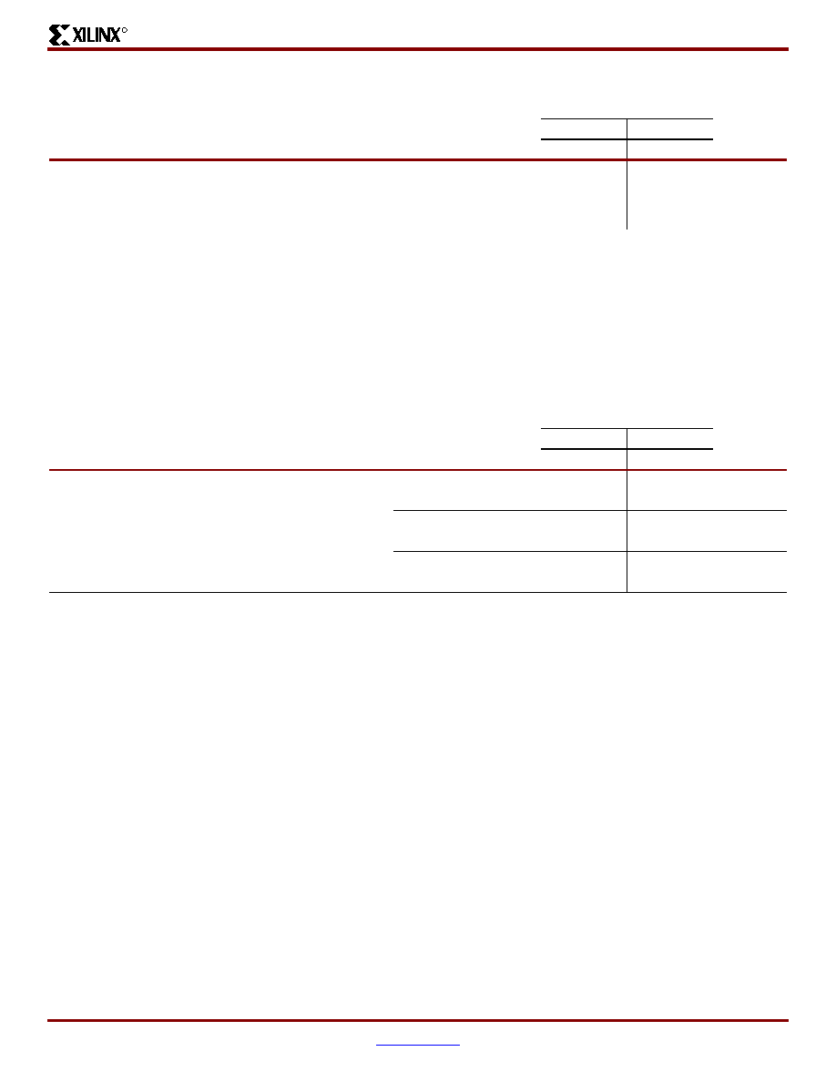
Global Clock Setup and Hold for LVTTL Standard, with DLL (Pin-to-Pin)
Global Clock Setup and Hold for LVTTL Standard, without DLL (Pin-to-Pin)
Symbol
Description
Device
Speed Grade
Units
-6
-5
Min
TPSDLL / TPHDLL
Input setup and hold time relative
to global clock input signal for
LVTTL standard, no delay, IFF,(1)
with DLL
All
1.7 / 0
1.9 / 0
ns
Notes:
1.
IFF = Input Flip-Flop or Latch
2.
Setup time is measured relative to the Global Clock input signal with the fastest route and the lightest load. Hold time is measured
relative to the Global Clock input signal with the slowest route and heaviest load.
3.
DLL output jitter is already included in the timing calculation.
4.
A zero hold time listing indicates no hold time or a negative hold time.
5.
For data input with different standards, adjust the setup time delay by the values shown in "IOB Input Delay Adjustments for Different
Standards," page 57. For a global clock input with standards other than LVTTL, adjust delays with values from the "I/O Standard
Symbol
Description
Device
Speed Grade
Units
-6
-5
Min
TPSFD / TPHFD
Input setup and hold time relative
to global clock input signal for
LVTTL standard, no delay, IFF,(1)
without DLL
XC2S15
2.2 / 0
2.7 / 0
ns
XC2S30
2.2 / 0
2.7 / 0
ns
XC2S50
2.2 / 0
2.7 / 0
ns
XC2S100
2.3 / 0
2.8 / 0
ns
XC2S150
2.4 / 0
2.9 / 0
ns
XC2S200
2.4 / 0
3.0 / 0
ns
Notes:
1.
IFF = Input Flip-Flop or Latch
2.
Setup time is measured relative to the Global Clock input signal with the fastest route and the lightest load. Hold time is measured
relative to the Global Clock input signal with the slowest route and heaviest load.
3.
A zero hold time listing indicates no hold time or a negative hold time.
4.
For data input with different standards, adjust the setup time delay by the values shown in "IOB Input Delay Adjustments for Different
Standards," page 57. For a global clock input with standards other than LVTTL, adjust delays with values from the "I/O Standard
相关PDF资料 |
PDF描述 |
|---|---|
| ABB92DHRT-S329 | CARD EXTEND PCI 184POS .050 3.3V |
| XA3S500E-4CPG132I | IC FPGA SPARTAN-3E 500K 132CSBGA |
| XC6SLX16-3FTG256C | IC FPGA SPARTAN 6 14K 256FTGBGA |
| XC6SLX16-3CSG225C | IC FPGA SPARTAN 6 14K 225CSGBGA |
| AMC31DRYN-S13 | CONN EDGECARD 62POS .100 EXTEND |
相关代理商/技术参数 |
参数描述 |
|---|---|
| XC2S150-5FG256C-ES | 制造商:Xilinx 功能描述: 制造商:Xilinx 功能描述:Field-Programmable Gate Array, 3888 Cell, 256 Pin, Plastic, BGA |
| XC2S150-5FG256I | 功能描述:IC FPGA 2.5V I-TEMP 256-FBGA RoHS:否 类别:集成电路 (IC) >> 嵌入式 - FPGA(现场可编程门阵列) 系列:Spartan®-II 标准包装:40 系列:Spartan® 6 LX LAB/CLB数:3411 逻辑元件/单元数:43661 RAM 位总计:2138112 输入/输出数:358 门数:- 电源电压:1.14 V ~ 1.26 V 安装类型:表面贴装 工作温度:-40°C ~ 100°C 封装/外壳:676-BGA 供应商设备封装:676-FBGA(27x27) |
| XC2S150-5FG456C | 功能描述:IC FPGA 2.5V 864 CLB'S 456-FBGA RoHS:否 类别:集成电路 (IC) >> 嵌入式 - FPGA(现场可编程门阵列) 系列:Spartan®-II 标准包装:40 系列:Spartan® 6 LX LAB/CLB数:3411 逻辑元件/单元数:43661 RAM 位总计:2138112 输入/输出数:358 门数:- 电源电压:1.14 V ~ 1.26 V 安装类型:表面贴装 工作温度:-40°C ~ 100°C 封装/外壳:676-BGA 供应商设备封装:676-FBGA(27x27) |
| XC2S150-5FG456I | 功能描述:IC FPGA 2.5V I-TEMP 456-FBGA RoHS:否 类别:集成电路 (IC) >> 嵌入式 - FPGA(现场可编程门阵列) 系列:Spartan®-II 标准包装:40 系列:Spartan® 6 LX LAB/CLB数:3411 逻辑元件/单元数:43661 RAM 位总计:2138112 输入/输出数:358 门数:- 电源电压:1.14 V ~ 1.26 V 安装类型:表面贴装 工作温度:-40°C ~ 100°C 封装/外壳:676-BGA 供应商设备封装:676-FBGA(27x27) |
| XC2S150-5FGG256C | 功能描述:IC SPARTAN-II FPGA 150K 256-FBGA RoHS:是 类别:集成电路 (IC) >> 嵌入式 - FPGA(现场可编程门阵列) 系列:Spartan®-II 标准包装:40 系列:Spartan® 6 LX LAB/CLB数:3411 逻辑元件/单元数:43661 RAM 位总计:2138112 输入/输出数:358 门数:- 电源电压:1.14 V ~ 1.26 V 安装类型:表面贴装 工作温度:-40°C ~ 100°C 封装/外壳:676-BGA 供应商设备封装:676-FBGA(27x27) |
发布紧急采购,3分钟左右您将得到回复。