参数资料
| 型号: | XC3S1000-4FT256I |
| 厂商: | Xilinx Inc |
| 文件页数: | 135/272页 |
| 文件大小: | 0K |
| 描述: | IC FPGA SPARTAN 3 256FTBGA |
| 标准包装: | 90 |
| 系列: | Spartan®-3 |
| LAB/CLB数: | 1920 |
| 逻辑元件/单元数: | 17280 |
| RAM 位总计: | 442368 |
| 输入/输出数: | 173 |
| 门数: | 1000000 |
| 电源电压: | 1.14 V ~ 1.26 V |
| 安装类型: | 表面贴装 |
| 工作温度: | -40°C ~ 100°C |
| 封装/外壳: | 256-LBGA |
| 供应商设备封装: | 256-FTBGA |
第1页第2页第3页第4页第5页第6页第7页第8页第9页第10页第11页第12页第13页第14页第15页第16页第17页第18页第19页第20页第21页第22页第23页第24页第25页第26页第27页第28页第29页第30页第31页第32页第33页第34页第35页第36页第37页第38页第39页第40页第41页第42页第43页第44页第45页第46页第47页第48页第49页第50页第51页第52页第53页第54页第55页第56页第57页第58页第59页第60页第61页第62页第63页第64页第65页第66页第67页第68页第69页第70页第71页第72页第73页第74页第75页第76页第77页第78页第79页第80页第81页第82页第83页第84页第85页第86页第87页第88页第89页第90页第91页第92页第93页第94页第95页第96页第97页第98页第99页第100页第101页第102页第103页第104页第105页第106页第107页第108页第109页第110页第111页第112页第113页第114页第115页第116页第117页第118页第119页第120页第121页第122页第123页第124页第125页第126页第127页第128页第129页第130页第131页第132页第133页第134页当前第135页第136页第137页第138页第139页第140页第141页第142页第143页第144页第145页第146页第147页第148页第149页第150页第151页第152页第153页第154页第155页第156页第157页第158页第159页第160页第161页第162页第163页第164页第165页第166页第167页第168页第169页第170页第171页第172页第173页第174页第175页第176页第177页第178页第179页第180页第181页第182页第183页第184页第185页第186页第187页第188页第189页第190页第191页第192页第193页第194页第195页第196页第197页第198页第199页第200页第201页第202页第203页第204页第205页第206页第207页第208页第209页第210页第211页第212页第213页第214页第215页第216页第217页第218页第219页第220页第221页第222页第223页第224页第225页第226页第227页第228页第229页第230页第231页第232页第233页第234页第235页第236页第237页第238页第239页第240页第241页第242页第243页第244页第245页第246页第247页第248页第249页第250页第251页第252页第253页第254页第255页第256页第257页第258页第259页第260页第261页第262页第263页第264页第265页第266页第267页第268页第269页第270页第271页第272页
Spartan-3 FPGA Family: Functional Description
DS099 (v3.1) June 27, 2013
Product Specification
22
Elements Within a Slice
All four slices have the following elements in common: two logic function generators, two storage elements, wide-function
multiplexers, carry logic, and arithmetic gates, as shown in Figure 12, page 24. Both the left-hand and right-hand slice pairs
use these elements to provide logic, arithmetic, and ROM functions. Besides these, the left-hand pair supports two
additional functions: storing data using Distributed RAM and shifting data with 16-bit registers. Figure 12 is a diagram of the
left-hand slice; therefore, it represents a superset of the elements and connections to be found in all slices. See Function
Generator, page 25 for more information.
The RAM-based function generator—also known as a Look-Up Table or LUT—is the main resource for implementing logic
functions. Furthermore, the LUTs in each left-hand slice pair can be configured as Distributed RAM or a 16-bit shift register.
For information on the former, refer to the chapter entitled “Using Look-Up Tables as Distributed RAM” in UG331; for
information on the latter, refer to the chapter entitled “Using Look-Up Tables as Shift Registers” in UG331. The function
generators located in the upper and lower portions of the slice are referred to as the "G" and "F", respectively.
The storage element, which is programmable as either a D-type flip-flop or a level-sensitive latch, provides a means for
synchronizing data to a clock signal, among other uses. The storage elements in the upper and lower portions of the slice
are called FFY and FFX, respectively.
Wide-function multiplexers effectively combine LUTs in order to permit more complex logic operations. Each slice has two of
these multiplexers with F5MUX in the lower portion of the slice and FiMUX in the upper portion. Depending on the slice,
FiMUX takes on the name F6MUX, F7MUX, or F8MUX. For more details on the multiplexers, refer to the chapter entitled
“Using Dedicated Multiplexers” in UG331.
The carry chain, together with various dedicated arithmetic logic gates, support fast and efficient implementations of math
operations. The carry chain enters the slice as CIN and exits as COUT. Five multiplexers control the chain: CYINIT, CY0F,
and CYMUXF in the lower portion as well as CY0G and CYMUXG in the upper portion. The dedicated arithmetic logic
includes the exclusive-OR gates XORG and XORF (upper and lower portions of the slice, respectively) as well as the AND
gates GAND and FAND (upper and lower portions, respectively). For more details on the carry logic, refer to the chapter
entitled “Using Carry and Arithmetic Logic” in UG331.
Main Logic Paths
Central to the operation of each slice are two nearly identical data paths, distinguished using the terms top and bottom. The
description that follows uses names associated with the bottom path. (The top path names appear in parentheses.) The
basic path originates at an interconnect-switch matrix outside the CLB. Four lines, F1 through F4 (or G1 through G4 on the
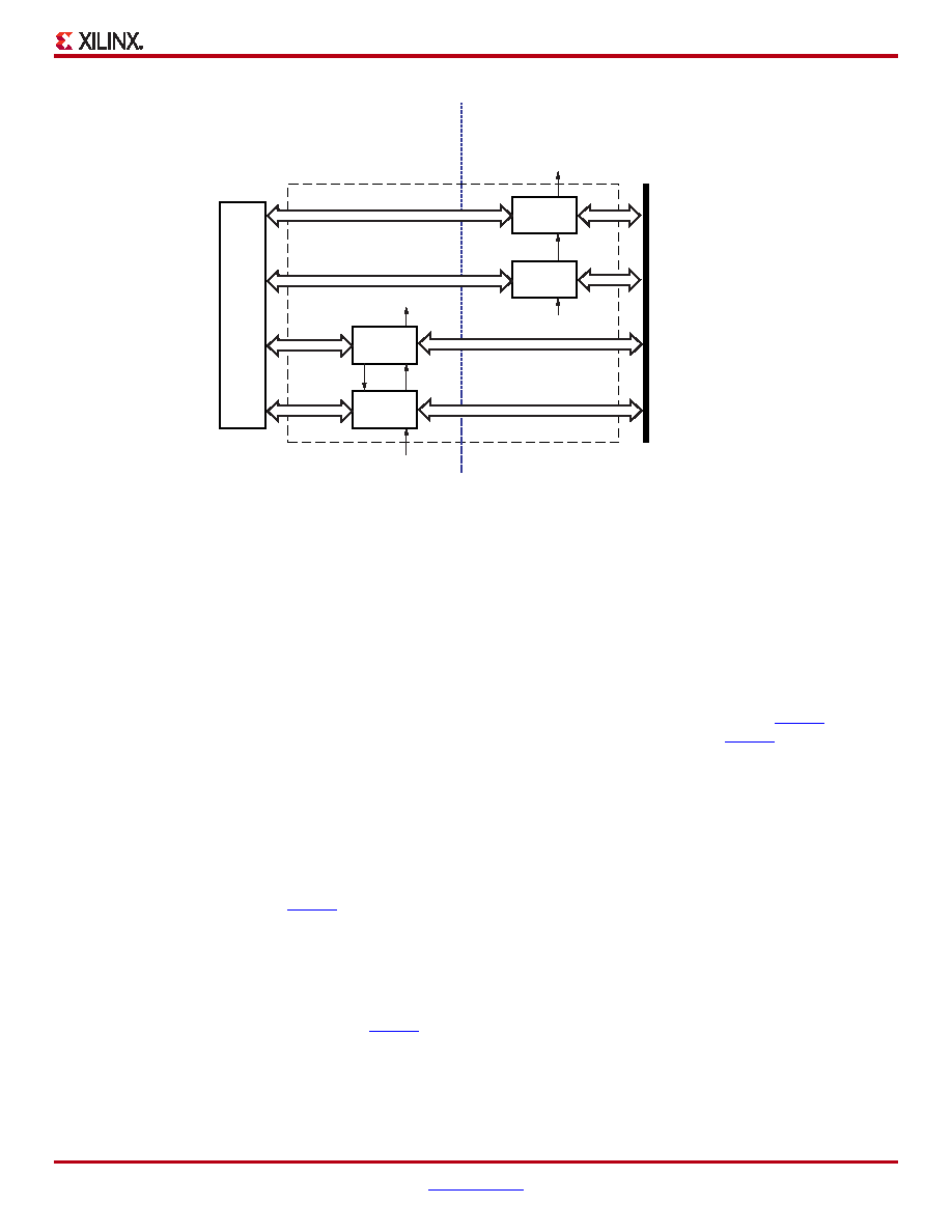
X-Ref Target - Figure 11
Figure 11: Arrangement of Slices within the CLB
DS099-2_05_082104
Interconnect
to Neighbors
Left-Hand SLICEM
(Logic or Distributed RAM
or Shift Register)
Right-Hand SLICEL
(Logic Only)
CIN
SLICE
X0Y1
SLICE
X0Y0
Switch
Matrix
COUT
CLB
COUT
SHIFTOUT
SHIFTIN
CIN
SLICE
X1Y1
SLICE
X1Y0
相关PDF资料 |
PDF描述 |
|---|---|
| XC3S1000-5FTG256C | SPARTAN-3A FPGA 1M 256-FTBGA |
| XC2V40-4FG256I | IC FPGA VIRTEX-II 256FGBGA |
| XC2V40-5FGG256C | IC FPGA VIRTEX-II 40K 256-FBGA |
| XC2V40-4FGG256I | IC FPGA VIRTEX-II 40K 256-FBGA |
| 3341-32BULK | CONN JACKSOCKET M2.5/4-40 0.50" |
相关代理商/技术参数 |
参数描述 |
|---|---|
| XC3S1000-4FTG256C | 功能描述:IC SPARTAN-3 FPGA 1M 256-FTBGA RoHS:是 类别:集成电路 (IC) >> 嵌入式 - FPGA(现场可编程门阵列) 系列:Spartan®-3 标准包装:60 系列:XP LAB/CLB数:- 逻辑元件/单元数:10000 RAM 位总计:221184 输入/输出数:244 门数:- 电源电压:1.71 V ~ 3.465 V 安装类型:表面贴装 工作温度:0°C ~ 85°C 封装/外壳:388-BBGA 供应商设备封装:388-FPBGA(23x23) 其它名称:220-1241 |
| XC3S1000-4FTG256C4124 | 制造商:Xilinx 功能描述: |
| XC3S1000-4FTG256I | 功能描述:SPARTAN-3A FPGA 1M STD 256-FTBGA RoHS:是 类别:集成电路 (IC) >> 嵌入式 - FPGA(现场可编程门阵列) 系列:Spartan®-3 标准包装:24 系列:ECP2 LAB/CLB数:1500 逻辑元件/单元数:12000 RAM 位总计:226304 输入/输出数:131 门数:- 电源电压:1.14 V ~ 1.26 V 安装类型:表面贴装 工作温度:0°C ~ 85°C 封装/外壳:208-BFQFP 供应商设备封装:208-PQFP(28x28) |
| XC3S1000-4PQ208C | 制造商:XILINX 制造商全称:XILINX 功能描述:Spartan-3 FPGA |
| XC3S1000-4PQ208I | 制造商:XILINX 制造商全称:XILINX 功能描述:Spartan-3 FPGA |
发布紧急采购,3分钟左右您将得到回复。