参数资料
| 型号: | XC3S1200E-5FGG400C |
| 厂商: | Xilinx Inc |
| 文件页数: | 220/227页 |
| 文件大小: | 0K |
| 描述: | IC FPGA SPARTAN-3E 1200K 400FBGA |
| 标准包装: | 60 |
| 系列: | Spartan®-3E |
| LAB/CLB数: | 2168 |
| 逻辑元件/单元数: | 19512 |
| RAM 位总计: | 516096 |
| 输入/输出数: | 304 |
| 门数: | 1200000 |
| 电源电压: | 1.14 V ~ 1.26 V |
| 安装类型: | 表面贴装 |
| 工作温度: | 0°C ~ 85°C |
| 封装/外壳: | 400-BGA |
| 供应商设备封装: | 400-FBGA(21x21) |
第1页第2页第3页第4页第5页第6页第7页第8页第9页第10页第11页第12页第13页第14页第15页第16页第17页第18页第19页第20页第21页第22页第23页第24页第25页第26页第27页第28页第29页第30页第31页第32页第33页第34页第35页第36页第37页第38页第39页第40页第41页第42页第43页第44页第45页第46页第47页第48页第49页第50页第51页第52页第53页第54页第55页第56页第57页第58页第59页第60页第61页第62页第63页第64页第65页第66页第67页第68页第69页第70页第71页第72页第73页第74页第75页第76页第77页第78页第79页第80页第81页第82页第83页第84页第85页第86页第87页第88页第89页第90页第91页第92页第93页第94页第95页第96页第97页第98页第99页第100页第101页第102页第103页第104页第105页第106页第107页第108页第109页第110页第111页第112页第113页第114页第115页第116页第117页第118页第119页第120页第121页第122页第123页第124页第125页第126页第127页第128页第129页第130页第131页第132页第133页第134页第135页第136页第137页第138页第139页第140页第141页第142页第143页第144页第145页第146页第147页第148页第149页第150页第151页第152页第153页第154页第155页第156页第157页第158页第159页第160页第161页第162页第163页第164页第165页第166页第167页第168页第169页第170页第171页第172页第173页第174页第175页第176页第177页第178页第179页第180页第181页第182页第183页第184页第185页第186页第187页第188页第189页第190页第191页第192页第193页第194页第195页第196页第197页第198页第199页第200页第201页第202页第203页第204页第205页第206页第207页第208页第209页第210页第211页第212页第213页第214页第215页第216页第217页第218页第219页当前第220页第221页第222页第223页第224页第225页第226页第227页
Spartan-3E FPGA Family: Functional Description
DS312 (v4.1) July 19, 2013
Product Specification
92
Stepping 0 Limitations when Reprogramming via
JTAG if FPGA Set for BPI Configuration
The FPGA can always be reprogrammed via the JTAG port,
regardless of the mode pin (M[2:0]) settings. However,
Stepping 0 devices have a minor limitation. If a Stepping 0
FPGA is set to configure in BPI mode and the FPGA is
attached to a parallel memory containing a valid FPGA
configuration file, then subsequent reconfigurations using
the JTAG port will fail. Potential workarounds include setting
the mode pins for JTAG configuration (M[2:0] = <1:0:1>) or
offsetting the initial memory location in Flash by 0x2000.
Stepping 1 devices fully support JTAG configuration even
when the FPGA mode pins are set for BPI mode.
In-System Programming Support
In a production application, the parallel Flash PROM is
usually preprogrammed before it is mounted on the printed
circuit board. In-system programming support is available
from third-party boundary-scan tool vendors and from some
third-party PROM programmers using a socket adapter with
attached wires. To gain access to the parallel Flash signals,
drive the FPGA’s PROG_B input Low with an open-drain
driver. This action places all FPGA I/O pins, including those
attached to the parallel Flash, in high-impedance (Hi-Z). If
the HSWAP input is Low, the I/Os have pull-up resistors to
the VCCO input on their respective I/O bank. The external
programming hardware then has direct access to the
parallel Flash pins. The programming access points are
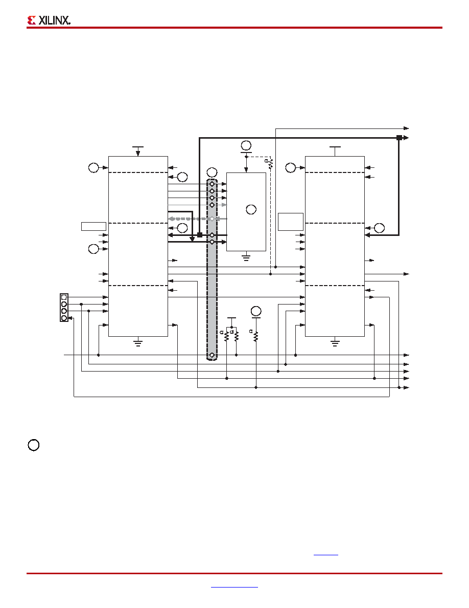
highlighted in the gray boxes in Figure 58 and Figure 59.
The FPGA itself can also be used as a parallel Flash PROM
programmer during development and test phases. Initially,
an FPGA-based programmer is downloaded into the FPGA
via JTAG. Then the FPGA performs the Flash PROM
programming algorithms and receives programming data
from the host via the FPGA’s JTAG interface. See the
Embedded System Tools Reference Manual.
Dynamically Loading Multiple Configuration
Images Using MultiBoot Option
For additional information, refer to the “Reconfiguration and
MultiBoot” chapter in UG332.
X-Ref Target - Figure 59
Figure 59: Daisy-Chaining from BPI Flash Mode
+2.5V
TDI
TDO
TMS
TCK
VCCINT
VCCAUX
+2.5V
HDC
CCLK
CSO_B
VCCO_1
INIT_B
CSI_B
D[7:0]
LDC1
LDC0
‘0’
A[16:0]
PROG_B
DONE
GND
VCCO_2
+1.2V
DQ[7:0]
A[n:0]
CE#
WE#
VCC
OE#
BYTE#
DQ[15:7]
GND
M2
M1
‘0’
‘1’
M0
HSWAP
VCCO_0
A
A[23:17]
P
LDC2
TDI
TDO
TMS
TCK
VCCINT
VCCAUX
CCLK
CSO_B
VCCO_1
INIT_B
CSI_B
D[7:0]
PROG_B
DONE
GND
VCCO_2
+1.2V
M2
M1
‘1’
M0
HSWAP
VCCO_0
P
VCCO_1
+2.5V
‘0’
VCCO_0
V
D
V
BPI Mode
Slave
Parallel
Mode
2.5V
JTAG
CCLK
D[7:0]
INIT_B
DONE
PROG_B
TCK
TMS
x8 or
x8/x16
Flash
PROM
PROG_B
Recommend
open-drain
driver
VCCO_0
TDI
TMS
TCK
TDO
RDWR_B
‘0’
CSO_B
RDWR_B
‘0’
BUSY
Spartan-3E
FPGA
Spartan-3E
FPGA
BUSY
I
33
0
4.
7
k
4.
7
k
Not available
in VQ100
package
DS312-2_50_082009
4.
7
k
I
相关PDF资料 |
PDF描述 |
|---|---|
| 0511171605 | CONN RETAINER FOR 16POS HOUSING |
| XC3S1200E-4FGG400I | IC FPGA SPARTAN-3E 1200K 400FBGA |
| GSC43DTEI | CONN EDGECARD 86POS .100 EYELET |
| XC6SLX25T-N3FGG484I | IC FPGA SPARTAN-6 484FBGA |
| XC3S1000-4FGG456I | SPARTAN-3A FPGA 1M STD 456-FBGA |
相关代理商/技术参数 |
参数描述 |
|---|---|
| XC3S1200E-5FGG400I | 制造商:XILINX 制造商全称:XILINX 功能描述:Spartan-3E FPGA Family |
| XC3S1200E-5FGG484C | 制造商:XILINX 制造商全称:XILINX 功能描述:Spartan-3E FPGA Family |
| XC3S1200E-5FGG484I | 制造商:XILINX 制造商全称:XILINX 功能描述:Spartan-3E FPGA Family |
| XC3S1200E-5FT256C | 制造商:Xilinx 功能描述:FPGA SPARTAN-3E 1.2M GATES 19512 CELLS 657MHZ 90NM 1.2V 256F - Trays |
| XC3S1200E-5FT256I | 制造商:XILINX 制造商全称:XILINX 功能描述:Spartan-3E FPGA Family |
发布紧急采购,3分钟左右您将得到回复。