参数资料
| 型号: | XC3S1200E-5FTG256C |
| 厂商: | Xilinx Inc |
| 文件页数: | 23/227页 |
| 文件大小: | 0K |
| 描述: | IC FPGA SPARTAN3E 1200K 256FTBGA |
| 标准包装: | 90 |
| 系列: | Spartan®-3E |
| LAB/CLB数: | 2168 |
| 逻辑元件/单元数: | 19512 |
| RAM 位总计: | 516096 |
| 输入/输出数: | 190 |
| 门数: | 1200000 |
| 电源电压: | 1.14 V ~ 1.26 V |
| 安装类型: | 表面贴装 |
| 工作温度: | 0°C ~ 85°C |
| 封装/外壳: | 256-LBGA |
| 供应商设备封装: | 256-FTBGA |
第1页第2页第3页第4页第5页第6页第7页第8页第9页第10页第11页第12页第13页第14页第15页第16页第17页第18页第19页第20页第21页第22页当前第23页第24页第25页第26页第27页第28页第29页第30页第31页第32页第33页第34页第35页第36页第37页第38页第39页第40页第41页第42页第43页第44页第45页第46页第47页第48页第49页第50页第51页第52页第53页第54页第55页第56页第57页第58页第59页第60页第61页第62页第63页第64页第65页第66页第67页第68页第69页第70页第71页第72页第73页第74页第75页第76页第77页第78页第79页第80页第81页第82页第83页第84页第85页第86页第87页第88页第89页第90页第91页第92页第93页第94页第95页第96页第97页第98页第99页第100页第101页第102页第103页第104页第105页第106页第107页第108页第109页第110页第111页第112页第113页第114页第115页第116页第117页第118页第119页第120页第121页第122页第123页第124页第125页第126页第127页第128页第129页第130页第131页第132页第133页第134页第135页第136页第137页第138页第139页第140页第141页第142页第143页第144页第145页第146页第147页第148页第149页第150页第151页第152页第153页第154页第155页第156页第157页第158页第159页第160页第161页第162页第163页第164页第165页第166页第167页第168页第169页第170页第171页第172页第173页第174页第175页第176页第177页第178页第179页第180页第181页第182页第183页第184页第185页第186页第187页第188页第189页第190页第191页第192页第193页第194页第195页第196页第197页第198页第199页第200页第201页第202页第203页第204页第205页第206页第207页第208页第209页第210页第211页第212页第213页第214页第215页第216页第217页第218页第219页第220页第221页第222页第223页第224页第225页第226页第227页
Spartan-3E FPGA Family: DC and Switching Characteristics
DS312 (v4.1) July 19, 2013
Product Specification
119
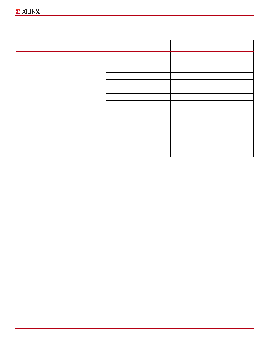
Quiescent Current Requirements
Table 79: Quiescent Supply Current Characteristics
Symbol
Description
Device
Typical
Commercial
Maximum(1)
Industrial
Maximum(1)
Units
ICCINTQ
Quiescent VCCINT supply current
XC3S100E
8
27
36
mA
XC3S250E
15
78
104
mA
XC3S500E
25
106
145
mA
XC3S1200E
50
259
324
mA
XC3S1600E
65
366
457
mA
ICCOQ
Quiescent VCCO supply current
XC3S100E
0.8
1.0
1.5
mA
XC3S250E
0.8
1.0
1.5
mA
XC3S500E
0.8
1.0
1.5
mA
XC3S1200E
1.5
2.0
2.5
mA
XC3S1600E
1.5
2.0
2.5
mA
ICCAUXQ
Quiescent VCCAUX supply current
XC3S100E
8
12
13
mA
XC3S250E
12
22
26
mA
XC3S500E
18
31
34
mA
XC3S1200E
35
52
59
mA
XC3S1600E
45
76
86
mA
Notes:
1.
The maximum numbers in this table indicate the minimum current each power rail requires in order for the FPGA to power-on successfully.
2.
The numbers in this table are based on the conditions set forth in Table 77.
3.
Quiescent supply current is measured with all I/O drivers in a high-impedance state and with all pull-up/pull-down resistors at the I/O pads
disabled. Typical values are characterized using typical devices at room temperature (TJ of 25°C at VCCINT = 1.2 V, VCCO = 3.3V, and VCCAUX
= 2.5V). The maximum limits are tested for each device at the respective maximum specified junction temperature and at maximum voltage
limits with VCCINT = 1.26V, VCCO = 3.465V, and VCCAUX = 2.625V. The FPGA is programmed with a “blank” configuration data file (i.e., a
design with no functional elements instantiated). For conditions other than those described above, (e.g., a design including functional
elements), measured quiescent current levels may be different than the values in the table. For more accurate estimates for a specific design,
use the Xilinx XPower tools.
4.
There are two recommended ways to estimate the total power consumption (quiescent plus dynamic) for a specific design: a) The
Spartan-3E XPower Estimator provides quick, approximate, typical estimates, and does not require a netlist of the design. b) XPower
Analyzer uses a netlist as input to provide maximum estimates as well as more accurate typical estimates.
相关PDF资料 |
PDF描述 |
|---|---|
| ACC60DRXH | CONN EDGECARD 120PS .100 DIP SLD |
| GCB100DHAR | CONN EDGECARD 200PS R/A .050 SLD |
| 3341-25 | CONN JACKSOCKET M2.5/M2 0.41" |
| XC3S1200E-4FTG256I | IC FPGA SPARTAN3E 1200K 256FTBGA |
| XC6SLX25T-N3CSG324C | IC FPGA SPARTAN-6 324CSBGA |
相关代理商/技术参数 |
参数描述 |
|---|---|
| XC3S1200E-5FTG256I | 制造商:XILINX 制造商全称:XILINX 功能描述:Spartan-3E FPGA Family |
| XC3S1200E-5PQ208C | 制造商:XILINX 制造商全称:XILINX 功能描述:Spartan-3E FPGA Family |
| XC3S1200E-5PQ208I | 制造商:XILINX 制造商全称:XILINX 功能描述:Spartan-3E FPGA Family |
| XC3S1200E-5PQG208C | 制造商:XILINX 制造商全称:XILINX 功能描述:Spartan-3E FPGA Family |
| XC3S1200E-5PQG208I | 制造商:XILINX 制造商全称:XILINX 功能描述:Spartan-3E FPGA Family |
发布紧急采购,3分钟左右您将得到回复。