参数资料
| 型号: | XC3S250E-4VQG100I |
| 厂商: | Xilinx Inc |
| 文件页数: | 153/227页 |
| 文件大小: | 0K |
| 描述: | IC FPGA SPARTAN-3E 250K 100-VQFP |
| 标准包装: | 90 |
| 系列: | Spartan®-3E |
| LAB/CLB数: | 612 |
| 逻辑元件/单元数: | 5508 |
| RAM 位总计: | 221184 |
| 输入/输出数: | 66 |
| 门数: | 250000 |
| 电源电压: | 1.14 V ~ 1.26 V |
| 安装类型: | 表面贴装 |
| 工作温度: | -40°C ~ 100°C |
| 封装/外壳: | 100-TQFP |
| 供应商设备封装: | 100-VQFP(14x14) |
| 其它名称: | 122-1715 XC3S250E-4VQG100I-ND |
第1页第2页第3页第4页第5页第6页第7页第8页第9页第10页第11页第12页第13页第14页第15页第16页第17页第18页第19页第20页第21页第22页第23页第24页第25页第26页第27页第28页第29页第30页第31页第32页第33页第34页第35页第36页第37页第38页第39页第40页第41页第42页第43页第44页第45页第46页第47页第48页第49页第50页第51页第52页第53页第54页第55页第56页第57页第58页第59页第60页第61页第62页第63页第64页第65页第66页第67页第68页第69页第70页第71页第72页第73页第74页第75页第76页第77页第78页第79页第80页第81页第82页第83页第84页第85页第86页第87页第88页第89页第90页第91页第92页第93页第94页第95页第96页第97页第98页第99页第100页第101页第102页第103页第104页第105页第106页第107页第108页第109页第110页第111页第112页第113页第114页第115页第116页第117页第118页第119页第120页第121页第122页第123页第124页第125页第126页第127页第128页第129页第130页第131页第132页第133页第134页第135页第136页第137页第138页第139页第140页第141页第142页第143页第144页第145页第146页第147页第148页第149页第150页第151页第152页当前第153页第154页第155页第156页第157页第158页第159页第160页第161页第162页第163页第164页第165页第166页第167页第168页第169页第170页第171页第172页第173页第174页第175页第176页第177页第178页第179页第180页第181页第182页第183页第184页第185页第186页第187页第188页第189页第190页第191页第192页第193页第194页第195页第196页第197页第198页第199页第200页第201页第202页第203页第204页第205页第206页第207页第208页第209页第210页第211页第212页第213页第214页第215页第216页第217页第218页第219页第220页第221页第222页第223页第224页第225页第226页第227页
Spartan-3E FPGA Family: Functional Description
DS312 (v4.1) July 19, 2013
Product Specification
31
The MULT_AND is useful for small multipliers. Larger
multipliers can be built using the dedicated 18x18 multiplier
blocks (see Dedicated Multipliers).
Storage Elements
The storage element, which is programmable as either a
D-type flip-flop or a level-sensitive transparent latch,
provides a means for synchronizing data to a clock signal,
among other uses. The storage elements in the top and
bottom portions of the slice are called FFY and FFX,
respectively. FFY has a fixed multiplexer on the D input
selecting either the combinatorial output Y or the bypass
signal BY. FFX selects between the combinatorial output X
or the bypass signal BX.
The functionality of a slice storage element is identical to
that described earlier for the I/O storage elements. All
signals have programmable polarity; the default active-High
function is described.
The control inputs R, S, CE, and C are all shared between
the two flip-flops in a slice.
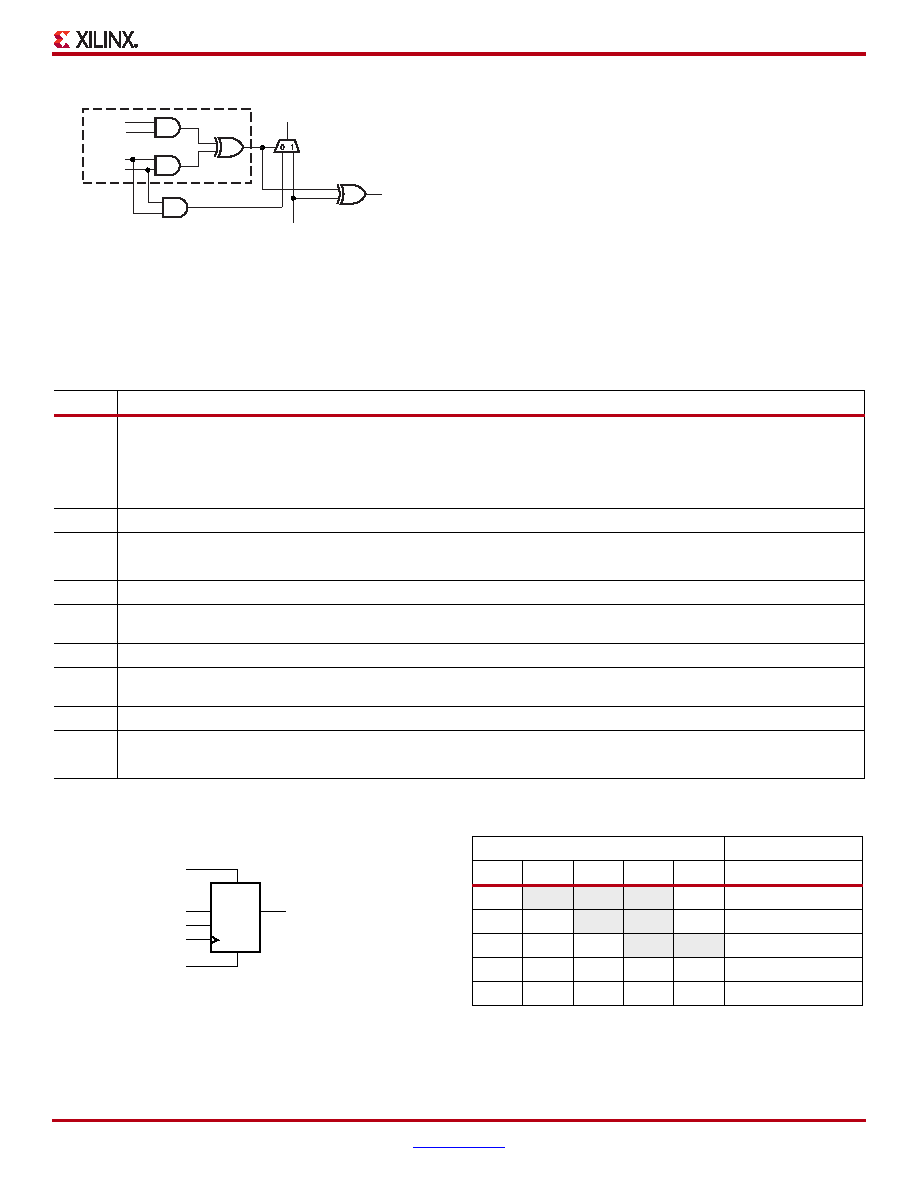
X-Ref Target - Figure 24
Figure 24: Using the MULT_AND for Multiplication in
Carry Logic
Bn+1
Am
Bn
Am+1
Pm+1
CIN
DS312-2_39_021305
COUT
LUT
MULT_AND
Table 15: Storage Element Signals
Signal
Description
D
Input. For a flip-flop data on the D input is loaded when R and S (or CLR and PRE) are Low and CE is High during the
Low-to-High clock transition. For a latch, Q reflects the D input while the gate (G) input and gate enable (GE) are High and R
and S (or CLR and PRE) are Low. The data on the D input during the High-to-Low gate transition is stored in the latch. The
data on the Q output of the latch remains unchanged as long as G or GE remains Low.
Q
Output. Toggles after the Low-to-High clock transition for a flip-flop and immediately for a latch.
C
Clock for edge-triggered flip-flops.
G
Gate for level-sensitive latches.
CE
Clock Enable for flip-flops.
GE
Gate Enable for latches.
S
Synchronous Set (Q = High). When the S input is High and R is Low, the flip-flop is set, output High, during the Low-to-High
clock (C) transition. A latch output is immediately set, output High.
R
Synchronous Reset (Q = Low); has precedence over Set.
PRE
Asynchronous Preset (Q = High). When the PRE input is High and CLR is Low, the flip-flop is set, output High, during the
Low-to-High clock (C) transition. A latch output is immediately set, output High.
CLR
Asynchronous Clear (Q = Low); has precedence over Preset to reset Q output Low
SR
CLB input for R, S, CLR, or PRE
REV
CLB input for opposite of SR. Must be asynchronous or synchronous to match SR.
X-Ref Target - Figure 25
Figure 25: FD Flip-Flop Component with Synchronous
Reset, Set, and Clock Enable
FDRSE
DQ
CE
C
R
S
DS312-2_40_021305
Table 16: FD Flip-Flop Functionality with Synchronous
Reset, Set, and Clock Enable
Inputs
Outputs
RS
CE
D
C
Q
1
X
↑
0
01
X
↑
1
00
0
X
No Change
00
11
↑
1
00
10
↑
0
相关PDF资料 |
PDF描述 |
|---|---|
| 24LC21T-I/SN | IC EEPROM 1KBIT 400KHZ 8SOIC |
| 24LC21A/SN | IC EEPROM 1KBIT 400KHZ 8SOIC |
| 24LC21AT/SN | IC EEPROM 1KBIT 400KHZ 8SOIC |
| 24LC21AT-I/SN | IC EEPROM 1KBIT 400KHZ 8SOIC |
| 24LC21A-I/SN | IC EEPROM 1KBIT 400KHZ 8SOIC |
相关代理商/技术参数 |
参数描述 |
|---|---|
| XC3S250E-5CP132C | 制造商:Xilinx 功能描述:FPGA SPARTAN-3E 250K GATES 5508 CELLS 657MHZ 90NM 1.2V 132CS - Trays |
| XC3S250E-5CP132I | 制造商:XILINX 制造商全称:XILINX 功能描述:Spartan-3E FPGA Family |
| XC3S250E-5CPG132C | 功能描述:IC FPGA SPARTAN-3E 250K 132CSBGA RoHS:是 类别:集成电路 (IC) >> 嵌入式 - FPGA(现场可编程门阵列) 系列:Spartan®-3E 标准包装:40 系列:Spartan® 6 LX LAB/CLB数:3411 逻辑元件/单元数:43661 RAM 位总计:2138112 输入/输出数:358 门数:- 电源电压:1.14 V ~ 1.26 V 安装类型:表面贴装 工作温度:-40°C ~ 100°C 封装/外壳:676-BGA 供应商设备封装:676-FBGA(27x27) |
| XC3S250E-5CPG132C4124 | 制造商:Xilinx 功能描述: |
| XC3S250E-5CPG132I | 制造商:XILINX 制造商全称:XILINX 功能描述:Spartan-3E FPGA Family |
发布紧急采购,3分钟左右您将得到回复。