参数资料
| 型号: | XC3S400-4TQG144I |
| 厂商: | Xilinx Inc |
| 文件页数: | 17/272页 |
| 文件大小: | 0K |
| 描述: | SPARTAN-3A FPGA 400K STD 144TQFP |
| 产品培训模块: | Extended Spartan 3A FPGA Family |
| 标准包装: | 60 |
| 系列: | Spartan®-3 |
| LAB/CLB数: | 896 |
| 逻辑元件/单元数: | 8064 |
| RAM 位总计: | 294912 |
| 输入/输出数: | 97 |
| 门数: | 400000 |
| 电源电压: | 1.14 V ~ 1.26 V |
| 安装类型: | 表面贴装 |
| 工作温度: | -40°C ~ 100°C |
| 封装/外壳: | 144-LQFP |
| 供应商设备封装: | 144-TQFP(20x20) |
第1页第2页第3页第4页第5页第6页第7页第8页第9页第10页第11页第12页第13页第14页第15页第16页当前第17页第18页第19页第20页第21页第22页第23页第24页第25页第26页第27页第28页第29页第30页第31页第32页第33页第34页第35页第36页第37页第38页第39页第40页第41页第42页第43页第44页第45页第46页第47页第48页第49页第50页第51页第52页第53页第54页第55页第56页第57页第58页第59页第60页第61页第62页第63页第64页第65页第66页第67页第68页第69页第70页第71页第72页第73页第74页第75页第76页第77页第78页第79页第80页第81页第82页第83页第84页第85页第86页第87页第88页第89页第90页第91页第92页第93页第94页第95页第96页第97页第98页第99页第100页第101页第102页第103页第104页第105页第106页第107页第108页第109页第110页第111页第112页第113页第114页第115页第116页第117页第118页第119页第120页第121页第122页第123页第124页第125页第126页第127页第128页第129页第130页第131页第132页第133页第134页第135页第136页第137页第138页第139页第140页第141页第142页第143页第144页第145页第146页第147页第148页第149页第150页第151页第152页第153页第154页第155页第156页第157页第158页第159页第160页第161页第162页第163页第164页第165页第166页第167页第168页第169页第170页第171页第172页第173页第174页第175页第176页第177页第178页第179页第180页第181页第182页第183页第184页第185页第186页第187页第188页第189页第190页第191页第192页第193页第194页第195页第196页第197页第198页第199页第200页第201页第202页第203页第204页第205页第206页第207页第208页第209页第210页第211页第212页第213页第214页第215页第216页第217页第218页第219页第220页第221页第222页第223页第224页第225页第226页第227页第228页第229页第230页第231页第232页第233页第234页第235页第236页第237页第238页第239页第240页第241页第242页第243页第244页第245页第246页第247页第248页第249页第250页第251页第252页第253页第254页第255页第256页第257页第258页第259页第260页第261页第262页第263页第264页第265页第266页第267页第268页第269页第270页第271页第272页
Spartan-3 FPGA Family: Pinout Descriptions
DS099 (v3.1) June 27, 2013
Product Specification
113
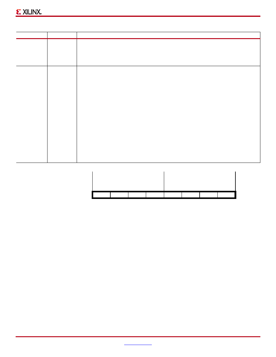
X-Ref Target - Figure 41
Parallel Configuration Modes (SelectMAP)
This section describes the dual-purpose configuration pins used during the Master and Slave Parallel configuration modes,
sometimes also called the SelectMAP modes. In both Master and Slave Parallel configuration modes, D0-D7 form the
byte-wide configuration data input. See Table 75 for Mode Select pin settings required for Parallel modes.
As shown in Figure 41, D0 is the most-significant bit while D7 is the least-significant bit. Bits D0-D3 form the high nibble of
the byte and bits D4-D7 form the low nibble.
In the Parallel configuration modes, both the VCCO_4 and VCCO_5 voltage supplies are required and must both equal the
voltage of the attached configuration device, typically either 2.5V or 3.3V.
Assert Low both the chip-select pin, CS_B, and the read/write control pin, RDWR_B, to write the configuration data byte
presented on the D0-D7 pins to the FPGA on a rising-edge of the configuration clock, CCLK. The order of CS_B and
RDWR_B does not matter, although RDWR_B must be asserted throughout the configuration process. If RDWR_B is
de-asserted during configuration, the FPGA aborts the configuration operation.
After configuration, these pins are available as general-purpose user I/O. However, the SelectMAP configuration interface is
optionally available for debugging and dynamic reconfiguration. To use these SelectMAP pins after configuration, set the
Persist bitstream generation option.
The Readback debugging option, for example, requires the Persist bitstream generation option. During Readback mode,
assert CS_B Low, along with RDWR_B High, to read a configuration data byte from the FPGA to the D0-D7 bus on a rising
CCLK edge. During Readback mode, D0-D7 are output pins.
In all the cases, the configuration data and control signals are synchronized to the rising edge of the CCLK clock signal.
Table 71: Dual-Purpose Pins Used in Master or Slave Serial Mode
Pin Name
Direction
Description
DIN
Input
Serial Data Input:
During the Master or Slave Serial configuration modes, DIN is the serial configuration data input, and
all data is synchronized to the rising CCLK edge. After configuration, this pin is available as a user I/O.
This signal is located in Bank 4 and its output voltage determined by VCCO_4.
The BitGen option Persist permits this pin to retain its configuration function in the User mode.
DOUT
Output
Serial Data Output:
In a multi-FPGA design where all the FPGAs use serial mode, connect the DOUT output of one
FPGA—in either Master or Slave Serial mode—to the DIN input of the next FPGA—in Slave Serial
mode—so that configuration data passes from one to the next, in daisy-chain fashion. This “daisy
chain” permits sequential configuration of multiple FPGAs.
This signal is located in Bank 4 and its output voltage determined by VCCO_4.
The BitGen option Persist permits this pin to retain its configuration function in the User mode.
INIT_B
Bidirectional
(open-drain)
Initializing Configuration Memory/Configuration Error:
Just after power is applied, the FPGA produces a Low-to-High transition on this pin indicating that
initialization (i.e., clearing) of the configuration memory has finished. Before entering the User mode,
this pin functions as an open-drain output, which requires a pull-up resistor in order to produce a High
logic level. In a multi-FPGA design, tie (wire AND) the INIT_B pins from all FPGAs together so that the
common node transitions High only after all of the FPGAs have been successfully initialized.
Externally holding this pin Low beyond the initialization phase delays the start of configuration. This
action stalls the FPGA at the configuration step just before the mode select pins are sampled.
During configuration, the FPGA indicates the occurrence of a data (i.e., CRC) error by asserting
INIT_B Low.
This signal is located in Bank 4 and its output voltage determined by VCCO_4.
The BitGen option Persist permits this pin to retain its configuration function in the User mode.
I/O Bank 4 (VCCO_4)
I/O Bank 5 (VCCO_5)
High Nibble
Low Nibble
Configuration Data Byte
D0
D1
D2
D3
D4
D5
D6
D7
0xFC =
1
0
(MSB)
(LSB)
Figure 41: Configuration Data Byte Mapping to D0-D7 Bits
相关PDF资料 |
PDF描述 |
|---|---|
| XC3S400-5TQG144C | SPARTAN-3A FPGA 400K 144-TQFP |
| EHHD15FFB | CONN DSUB 15PIN FMAL-FMAL BLACK |
| XC6SLX9-L1CPG196I | IC FPAG SPARTAN 6 9K 196CPGBGA |
| XA3S250E-4TQG144I | IC FPGA SPARTAN-3E 250K 144-TQFP |
| XA3S250E-4CPG132I | IC FPGA SPARTAN-3E 250K 132CSBGA |
相关代理商/技术参数 |
参数描述 |
|---|---|
| XC3S400-4TQG14C | 制造商:Xilinx 功能描述: |
| XC3S400-4VQ100C | 制造商:XILINX 制造商全称:XILINX 功能描述:Spartan-3 FPGA |
| XC3S400-4VQ100I | 制造商:XILINX 制造商全称:XILINX 功能描述:Spartan-3 FPGA |
| XC3S400-4VQG100C | 制造商:XILINX 制造商全称:XILINX 功能描述:Spartan-3 FPGA Family: Complete Data Sheet |
| XC3S400-4VQG100I | 制造商:XILINX 制造商全称:XILINX 功能描述:Spartan-3 FPGA Family: Complete Data Sheet |
发布紧急采购,3分钟左右您将得到回复。