参数资料
| 型号: | XC3S400-4TQG144I |
| 厂商: | Xilinx Inc |
| 文件页数: | 231/272页 |
| 文件大小: | 0K |
| 描述: | SPARTAN-3A FPGA 400K STD 144TQFP |
| 产品培训模块: | Extended Spartan 3A FPGA Family |
| 标准包装: | 60 |
| 系列: | Spartan®-3 |
| LAB/CLB数: | 896 |
| 逻辑元件/单元数: | 8064 |
| RAM 位总计: | 294912 |
| 输入/输出数: | 97 |
| 门数: | 400000 |
| 电源电压: | 1.14 V ~ 1.26 V |
| 安装类型: | 表面贴装 |
| 工作温度: | -40°C ~ 100°C |
| 封装/外壳: | 144-LQFP |
| 供应商设备封装: | 144-TQFP(20x20) |
第1页第2页第3页第4页第5页第6页第7页第8页第9页第10页第11页第12页第13页第14页第15页第16页第17页第18页第19页第20页第21页第22页第23页第24页第25页第26页第27页第28页第29页第30页第31页第32页第33页第34页第35页第36页第37页第38页第39页第40页第41页第42页第43页第44页第45页第46页第47页第48页第49页第50页第51页第52页第53页第54页第55页第56页第57页第58页第59页第60页第61页第62页第63页第64页第65页第66页第67页第68页第69页第70页第71页第72页第73页第74页第75页第76页第77页第78页第79页第80页第81页第82页第83页第84页第85页第86页第87页第88页第89页第90页第91页第92页第93页第94页第95页第96页第97页第98页第99页第100页第101页第102页第103页第104页第105页第106页第107页第108页第109页第110页第111页第112页第113页第114页第115页第116页第117页第118页第119页第120页第121页第122页第123页第124页第125页第126页第127页第128页第129页第130页第131页第132页第133页第134页第135页第136页第137页第138页第139页第140页第141页第142页第143页第144页第145页第146页第147页第148页第149页第150页第151页第152页第153页第154页第155页第156页第157页第158页第159页第160页第161页第162页第163页第164页第165页第166页第167页第168页第169页第170页第171页第172页第173页第174页第175页第176页第177页第178页第179页第180页第181页第182页第183页第184页第185页第186页第187页第188页第189页第190页第191页第192页第193页第194页第195页第196页第197页第198页第199页第200页第201页第202页第203页第204页第205页第206页第207页第208页第209页第210页第211页第212页第213页第214页第215页第216页第217页第218页第219页第220页第221页第222页第223页第224页第225页第226页第227页第228页第229页第230页当前第231页第232页第233页第234页第235页第236页第237页第238页第239页第240页第241页第242页第243页第244页第245页第246页第247页第248页第249页第250页第251页第252页第253页第254页第255页第256页第257页第258页第259页第260页第261页第262页第263页第264页第265页第266页第267页第268页第269页第270页第271页第272页
Spartan-3 FPGA Family: DC and Switching Characteristics
DS099 (v3.1) June 27, 2013
Product Specification
61
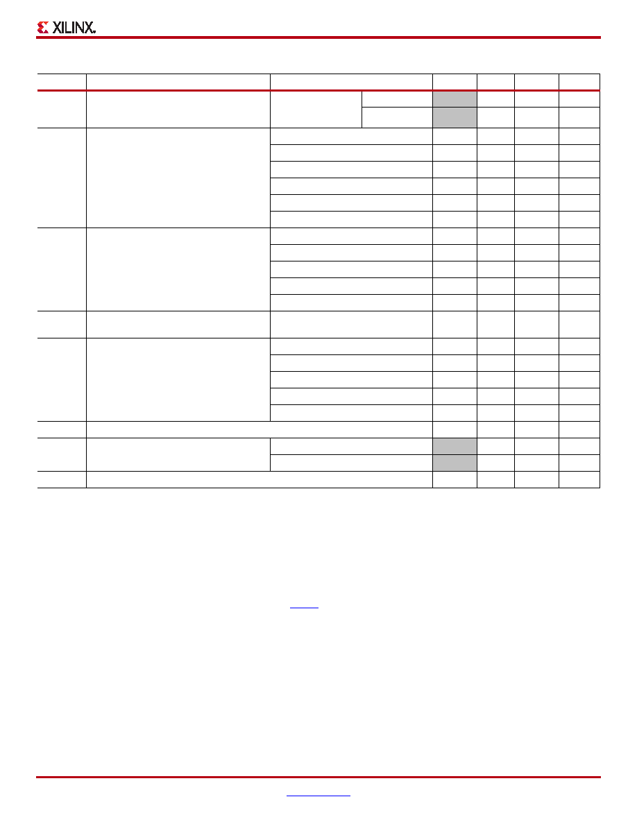
Table 33: General DC Characteristics of User I/O, Dual-Purpose, and Dedicated Pins
Symbol
Description
Test Conditions
Min
Typ
Max
Units
Leakage current at User I/O,
Dual-Purpose, and Dedicated pins
Driver is Hi-Z, VIN =
0V or VCCO max,
sample-tested
VCCO ≥ 3.0V
–-
±25
μA
VCCO < 3.0V
–-
±10
μA
IRPU(3)
Current through pull-up resistor at User I/O,
Dual-Purpose, and Dedicated pins
VIN = 0V, VCCO = 3.3V
–0.84
-
–2.35
mA
VIN = 0V, VCCO = 3.0V
–0.69
-
–1.99
mA
VIN = 0V, VCCO = 2.5V
–0.47
-
–1.41
mA
VIN = 0V, VCCO = 1.8V
–0.21
-
–0.69
mA
VIN = 0V, VCCO = 1.5V
–0.13
-
–0.43
mA
VIN = 0V, VCCO = 1.2V
–0.06
-
–0.22
mA
RPU(3)
Equivalent resistance of pull-up resistor at
User I/O, Dual-Purpose, and Dedicated
pins, derived from IRPU
VCCO = 3.0V to 3.465V
1.27
-
4.11
k
Ω
VCCO = 2.3V to 2.7V
1.15
-
3.25
k
Ω
VCCO = 1.7V to 1.9V
2.45
-
9.10
k
Ω
VCCO = 1.4V to 1.6V
3.25
-
12.10
k
Ω
VCCO = 1.14 to 1.26V
5.15
-
21.00
k
Ω
IRPD(3)
Current through pull-down resistor at User
I/O, Dual-Purpose, and Dedicated pins
VIN = VCCO
0.37
-
1.67
mA
RPD(3)
Equivalent resistance of pull-down resistor
at User I/O, Dual-Purpose, and Dedicated
pins, driven from IRPD
VIN = VCCO = 3.0V to 3.465V
1.75
-
9.35
k
Ω
VIN = VCCO = 2.3V to 2.7V
1.35
-
7.30
k
Ω
VIN = VCCO = 1.7V to 1.9V
1.00
-
5.15
k
Ω
VIN = VCCO = 1.4V to 1.6V
0.85
-
4.35
k
Ω
VIN = VCCO = 1.14 to 1.26V
0.68
-
3.465
k
Ω
RDCI
Value of external reference resistor to support DCI I/O standards
20
-
100
Ω
IREF
VREF current per pin
VCCO ≥ 3.0V
–-
±25
μA
VCCO < 3.0V
–-
±10
μA
CIN
Input capacitance
3
-
10
pF
Notes:
1.
The numbers in this table are based on the conditions set forth in Table 32.
2.
The IL specification applies to every I/O pin throughout power-on as long as the voltage on that pin stays between the absolute VIN minimum
and maximum values (Table 28). For hot-swap applications, at the time of card connection, be sure to keep all I/O voltages within this range
before applying VCCO power. Consider applying VCCO power before connecting the signal lines, to avoid turning on the ESD protection
diodes, shown in Module 2: Figure 7, page 11. When the FPGA is completely unpowered, the I/O pins are high impedance, but there is a
path through the upper and lower ESD protection diodes.
3.
This parameter is based on characterization. The pull-up resistance RPU = VCCO / IRPU. The pull-down resistance RPD =VIN /IRPD.
Spartan-3 family values for both resistances are stronger than they have been for previous FPGA families.
4.
For single-ended signals that are placed on a differential-capable I/O, VIN of –0.2V to –0.3V is supported but can cause increased leakage
between the two pins. See the Parasitic Leakage section in UG331, Spartan-3 Generation FPGA User Guide.
相关PDF资料 |
PDF描述 |
|---|---|
| XC3S400-5TQG144C | SPARTAN-3A FPGA 400K 144-TQFP |
| EHHD15FFB | CONN DSUB 15PIN FMAL-FMAL BLACK |
| XC6SLX9-L1CPG196I | IC FPAG SPARTAN 6 9K 196CPGBGA |
| XA3S250E-4TQG144I | IC FPGA SPARTAN-3E 250K 144-TQFP |
| XA3S250E-4CPG132I | IC FPGA SPARTAN-3E 250K 132CSBGA |
相关代理商/技术参数 |
参数描述 |
|---|---|
| XC3S400-4TQG14C | 制造商:Xilinx 功能描述: |
| XC3S400-4VQ100C | 制造商:XILINX 制造商全称:XILINX 功能描述:Spartan-3 FPGA |
| XC3S400-4VQ100I | 制造商:XILINX 制造商全称:XILINX 功能描述:Spartan-3 FPGA |
| XC3S400-4VQG100C | 制造商:XILINX 制造商全称:XILINX 功能描述:Spartan-3 FPGA Family: Complete Data Sheet |
| XC3S400-4VQG100I | 制造商:XILINX 制造商全称:XILINX 功能描述:Spartan-3 FPGA Family: Complete Data Sheet |
发布紧急采购,3分钟左右您将得到回复。