- 您现在的位置:买卖IC网 > PDF目录205935 > XC5204-6TQ144C (XILINX INC) Field Programmable Gate Arrays PDF资料下载
参数资料
| 型号: | XC5204-6TQ144C |
| 厂商: | XILINX INC |
| 元件分类: | FPGA |
| 英文描述: | Field Programmable Gate Arrays |
| 中文描述: | FPGA, 120 CLBS, 4000 GATES, 83 MHz, PQFP144 |
| 封装: | PLASTIC, TQFP-144 |
| 文件页数: | 3/73页 |
| 文件大小: | 598K |
| 代理商: | XC5204-6TQ144C |
第1页第2页当前第3页第4页第5页第6页第7页第8页第9页第10页第11页第12页第13页第14页第15页第16页第17页第18页第19页第20页第21页第22页第23页第24页第25页第26页第27页第28页第29页第30页第31页第32页第33页第34页第35页第36页第37页第38页第39页第40页第41页第42页第43页第44页第45页第46页第47页第48页第49页第50页第51页第52页第53页第54页第55页第56页第57页第58页第59页第60页第61页第62页第63页第64页第65页第66页第67页第68页第69页第70页第71页第72页第73页
R
November 5, 1998 (Version 5.2)
7-93
XC5200 Series Field Programmable Gate Arrays
7
to Vcc. The configurable pull-down resistor is an n-channel
transistor that pulls to Ground.
The value of these resistors is 20 k
100 k. This high
value makes them unsuitable as wired-AND pull-up resis-
tors.
The pull-up resistors for most user-programmable IOBs are
active during the configuration process. See Table 13 on
page 124 for a list of pins with pull-ups active before and
during configuration.
After configuration, voltage levels of unused pads, bonded
or unbonded, must be valid logic levels, to reduce noise
sensitivity and avoid excess current. Therefore, by default,
unused pads are configured with the internal pull-up resis-
tor active. Alternatively, they can be individually configured
with the pull-down resistor, or as a driven output, or to be
driven by an external source. To activate the internal
pull-up, attach the PULLUP library component to the net
attached to the pad. To activate the internal pull-down,
attach the PULLDOWN library component to the net
attached to the pad.
JTAG Support
Embedded logic attached to the IOBs contains test struc-
tures compatible with IEEE Standard 1149.1 for boundary
scan testing, simplifying board-level testing. More informa-
tion is provided in “Boundary Scan” on page 98.
Oscillator
XC5200 devices include an internal oscillator. This oscilla-
tor is used to clock the power-on time-out, clear configura-
tion memory, and source CCLK in Master configuration
modes. The oscillator runs at a nominal 12 MHz frequency
that varies with process, Vcc, and temperature. The output
CCLK frequency is selectable as 1 MHz (default), 6 MHz,
or 12 MHz.
The XC5200 oscillator divides the internal 12-MHz clock or
a user clock. The user then has the choice of dividing by 4,
16, 64, or 256 for the “OSC1” output and dividing by 2, 8,
32, 128, 1024, 4096, 16384, or 65536 for the “OSC2” out-
put. The division is specified via a “DIVIDEn_BY=x”
attribute on the symbol, where n=1 for OSC1, or n=2 for
OSC2. These frequencies can vary by as much as -50% or
+ 50%.
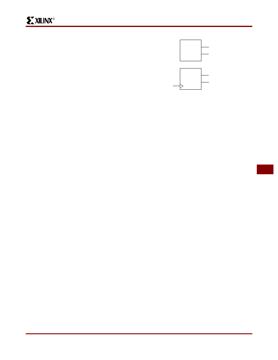
The OSC5 macro is used where an internal oscillator is
required. The CK_DIV macro is applicable when a user
clock input is specified (see Figure 13).
VersaBlock Routing
The General Routing Matrix (GRM) connects to the
Versa-Block via 24 bidirectional ports (M0-M23). Excluding
direct connections, global nets, and 3-statable Longlines,
all VersaBlock inputs and outputs connect to the GRM via
these 24 ports. Four 3-statable unidirectional signals
(TQ0-TQ3) drive out of the VersaBlock directly onto the
horizontal and vertical Longlines. Two horizontal global
nets and two vertical global nets connect directly to every
CLB clock pin; they can connect to other CLB inputs via the
GRM. Each CLB also has four unidirectional direct con-
nects to each of its four neighboring CLBs. These direct
connects can also feed directly back to the CLB (see
In addition, each CLB has 16 direct inputs, four direct con-
nections from each of the neighboring CLBs. These direct
connections
provide
high-speed
local
routing
that
bypasses the GRM.
Local Interconnect Matrix
The Local Interconnect Matrix (LIM) is built from input and
output multiplexers. The 13 CLB outputs (12 LC outputs
plus a Vcc/GND signal) connect to the eight VersaBlock
outputs via the output multiplexers, which consist of eight
fully
populated
13-to-1
multiplexers.
Of
the
eight
VersaBlock outputs, four signals drive each neighboring
CLB directly, and provide a direct feedback path to the input
multiplexers. The four remaining multiplexer outputs can
drive the GRM through four TBUFs (TQ0-TQ3). All eight
multiplexer outputs can connect to the GRM through the
bidirectional M0-M23 signals. All eight signals also connect
to the input multiplexers and are potential inputs to that
CLB.
OSCS
CK_DIV
OSC1
OSC2
5200_14
Figure 13: XC5200 Oscillator Macros
相关PDF资料 |
PDF描述 |
|---|---|
| XC5206-3BG225C | Field Programmable Gate Arrays |
| XC5206-3BG352C | Field Programmable Gate Arrays |
| XC5206-3HQ208C | Field Programmable Gate Arrays |
| XC5206-3HQ240C | Field Programmable Gate Arrays |
| XC5206-3PG156C | Field Programmable Gate Arrays |
相关代理商/技术参数 |
参数描述 |
|---|---|
| XC5204-6TQ144I | 制造商:Xilinx 功能描述: |
| XC5204-6TQ176C | 制造商:XILINX 制造商全称:XILINX 功能描述:Field Programmable Gate Arrays |
| XC5204-6VQ100C | 功能描述:IC FPGA 120 CLB'S 100-VQFP RoHS:否 类别:集成电路 (IC) >> 嵌入式 - FPGA(现场可编程门阵列) 系列:XC5200 产品变化通告:XC4000(E,L) Discontinuation 01/April/2002 标准包装:24 系列:XC4000E/X LAB/CLB数:100 逻辑元件/单元数:238 RAM 位总计:3200 输入/输出数:80 门数:3000 电源电压:4.5 V ~ 5.5 V 安装类型:表面贴装 工作温度:-40°C ~ 100°C 封装/外壳:120-BCBGA 供应商设备封装:120-CPGA(34.55x34.55) |
| XC5204-6VQ100I | 制造商:Xilinx 功能描述: |
| XC5204-6VQ64C | 制造商:XILINX 制造商全称:XILINX 功能描述:Field Programmable Gate Arrays |
发布紧急采购,3分钟左右您将得到回复。