参数资料
| 型号: | XC6SLX45T-2FG484I |
| 厂商: | Xilinx Inc |
| 文件页数: | 49/89页 |
| 文件大小: | 0K |
| 描述: | IC FPGA SPARTAN 6 484FGGBGA |
| 标准包装: | 60 |
| 系列: | Spartan® 6 LXT |
| LAB/CLB数: | 3411 |
| 逻辑元件/单元数: | 43661 |
| RAM 位总计: | 2138112 |
| 输入/输出数: | 296 |
| 电源电压: | 1.14 V ~ 1.26 V |
| 安装类型: | 表面贴装 |
| 工作温度: | -40°C ~ 100°C |
| 封装/外壳: | 484-BBGA |
| 供应商设备封装: | 484-FBGA |
第1页第2页第3页第4页第5页第6页第7页第8页第9页第10页第11页第12页第13页第14页第15页第16页第17页第18页第19页第20页第21页第22页第23页第24页第25页第26页第27页第28页第29页第30页第31页第32页第33页第34页第35页第36页第37页第38页第39页第40页第41页第42页第43页第44页第45页第46页第47页第48页当前第49页第50页第51页第52页第53页第54页第55页第56页第57页第58页第59页第60页第61页第62页第63页第64页第65页第66页第67页第68页第69页第70页第71页第72页第73页第74页第75页第76页第77页第78页第79页第80页第81页第82页第83页第84页第85页第86页第87页第88页第89页
Spartan-6 FPGA Data Sheet: DC and Switching Characteristics
DS162 (v3.0) October 17, 2011
Product Specification
53
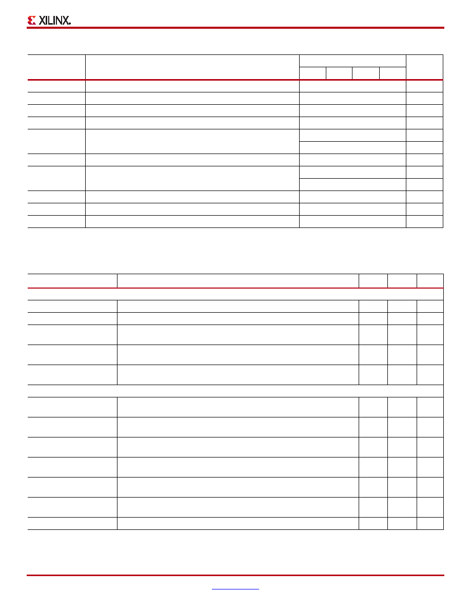
Table 45: Device DNA Interface Port Switching Characteristics
Symbol
Description
Speed Grade
Units
-3
-3N
-2
-1L
TDNASSU
Setup time on SHIFT before the rising edge of CLK
7
ns, Min
TDNASH
Hold time on SHIFT after the rising edge of CLK
1
ns, Min
TDNADSU
Setup time on DIN before the rising edge of CLK
7
ns, Min
TDNADH
Hold time on DIN after the rising edge of CLK
1
ns, Min
TDNARSU
Setup time on READ before the rising edge of CLK
7ns, Min
1,000
ns, Max
TDNARH
Hold time on READ after the rising edge of CLK
1
ns, Min
TDNADCKO
Clock-to-output delay on DOUT after rising edge of CLK
0.5
ns, Min
6ns, Max
TDNACLKF(2)
CLK frequency
2
MHz, Max
TDNACLKL
CLK Low time
50
ns, Min
TDNACLKH
CLK High time
50
ns, Min
Notes:
1.
The minimum READ pulse width is 8 ns, the maximum READ pulse width is 1 s.
2.
Also applies to TCK when reading DNA through the boundary-scan port.
Table 46: Suspend Mode Switching Characteristics
Symbol
Description
Min
Max
Units
Entering Suspend Mode
TSUSPENDHIGH_AWAKE
Rising edge of SUSPEND pin to falling edge of AWAKE pin without glitch filter
2.5
14
ns
TSUSPENDFILTER
Adjustment to SUSPEND pin rising edge parameters when glitch filter enabled
31
430
ns
TSUSPEND_GWE
Rising edge of SUSPEND pin until FPGA output pins drive their defined
SUSPEND constraint behavior (without glitch filter)
–15
ns
TSUSPEND_GTS
Rising edge of SUSPEND pin to write-protect lock on all writable clocked
elements (without glitch filter)
–15
ns
TSUSPEND_DISABLE
Rising edge of the SUSPEND pin to FPGA input pins and interconnect
disabled (without glitch filter)
–
1500
ns
Exiting Suspend Mode
TSUSPENDLOW_AWAKE
Falling edge of the SUSPEND pin to rising edge of the AWAKE pin. Does not
include DCM or PLL lock time.
775
s
TSUSPEND_ENABLE
Falling edge of the SUSPEND pin to FPGA input pins and interconnect re-
enabled
741
s
TAWAKE_GWE1
Rising edge of the AWAKE pin until write-protect lock released on all writable
clocked elements, using sw_clk:InternalClock and sw_gwe_cycle:1.
–80
ns
TAWAKE_GWE512
Rising edge of the AWAKE pin until write-protect lock released on all writable
clocked elements, using sw_clk:InternalClock and sw_gwe_cycle:512.
–20.5
s
TAWAKE_GTS1
Rising edge of the AWAKE pin until outputs return to the behavior described in
the FPGA application, using sw_clk:InternalClock and sw_gts_cycle:1.
–80
ns
TAWAKE_GTS512
Rising edge of the AWAKE pin until outputs return to the behavior described in
the FPGA application, using sw_clk:InternalClock and sw_gts_cycle:512.
–20.5
s
TSCP_AWAKE
Rising edge of SCP pins to rising edge of AWAKE pin
7
75
s
相关PDF资料 |
PDF描述 |
|---|---|
| XC6SLX45T-2FGG484I | IC FPGA SPARTAN 6 43K 484FGGBGA |
| 25LC080D-E/ST | IC SRL EEPROM 1KX8 2.5V 8-TSSOP |
| 25LC080C-E/MS | IC SRL EEPROM 1KX8 2.5V 8-MSOP |
| XC6SLX45T-N3CSG484I | IC FPGA SPARTAN-6 484CSBGA |
| 25AA320AXT-I/ST | IC EEPROM 32KBIT 10MHZ 8TSSOP |
相关代理商/技术参数 |
参数描述 |
|---|---|
| XC6SLX45T-2FGG484C | 功能描述:IC FPGA SPARTAN 6 43K 484FGGBGA RoHS:是 类别:集成电路 (IC) >> 嵌入式 - FPGA(现场可编程门阵列) 系列:Spartan® 6 LXT 标准包装:60 系列:XP LAB/CLB数:- 逻辑元件/单元数:10000 RAM 位总计:221184 输入/输出数:244 门数:- 电源电压:1.71 V ~ 3.465 V 安装类型:表面贴装 工作温度:0°C ~ 85°C 封装/外壳:388-BBGA 供应商设备封装:388-FPBGA(23x23) 其它名称:220-1241 |
| XC6SLX45T-2FGG484CES9982 | 制造商:Xilinx 功能描述: |
| XC6SLX45T-2FGG484I | 功能描述:IC FPGA SPARTAN 6 43K 484FGGBGA RoHS:是 类别:集成电路 (IC) >> 嵌入式 - FPGA(现场可编程门阵列) 系列:Spartan® 6 LXT 标准包装:40 系列:Spartan® 6 LX LAB/CLB数:3411 逻辑元件/单元数:43661 RAM 位总计:2138112 输入/输出数:358 门数:- 电源电压:1.14 V ~ 1.26 V 安装类型:表面贴装 工作温度:-40°C ~ 100°C 封装/外壳:676-BGA 供应商设备封装:676-FBGA(27x27) |
| XC6SLX45T-2FGG676C | 制造商:Xilinx 功能描述: |
| XC6SLX45T-2FGG676I | 制造商:Xilinx 功能描述: |
发布紧急采购,3分钟左右您将得到回复。