参数资料
| 型号: | XC6SLX45T-2FG484I |
| 厂商: | Xilinx Inc |
| 文件页数: | 54/89页 |
| 文件大小: | 0K |
| 描述: | IC FPGA SPARTAN 6 484FGGBGA |
| 标准包装: | 60 |
| 系列: | Spartan® 6 LXT |
| LAB/CLB数: | 3411 |
| 逻辑元件/单元数: | 43661 |
| RAM 位总计: | 2138112 |
| 输入/输出数: | 296 |
| 电源电压: | 1.14 V ~ 1.26 V |
| 安装类型: | 表面贴装 |
| 工作温度: | -40°C ~ 100°C |
| 封装/外壳: | 484-BBGA |
| 供应商设备封装: | 484-FBGA |
第1页第2页第3页第4页第5页第6页第7页第8页第9页第10页第11页第12页第13页第14页第15页第16页第17页第18页第19页第20页第21页第22页第23页第24页第25页第26页第27页第28页第29页第30页第31页第32页第33页第34页第35页第36页第37页第38页第39页第40页第41页第42页第43页第44页第45页第46页第47页第48页第49页第50页第51页第52页第53页当前第54页第55页第56页第57页第58页第59页第60页第61页第62页第63页第64页第65页第66页第67页第68页第69页第70页第71页第72页第73页第74页第75页第76页第77页第78页第79页第80页第81页第82页第83页第84页第85页第86页第87页第88页第89页
Spartan-6 FPGA Data Sheet: DC and Switching Characteristics
DS162 (v3.0) October 17, 2011
Product Specification
58
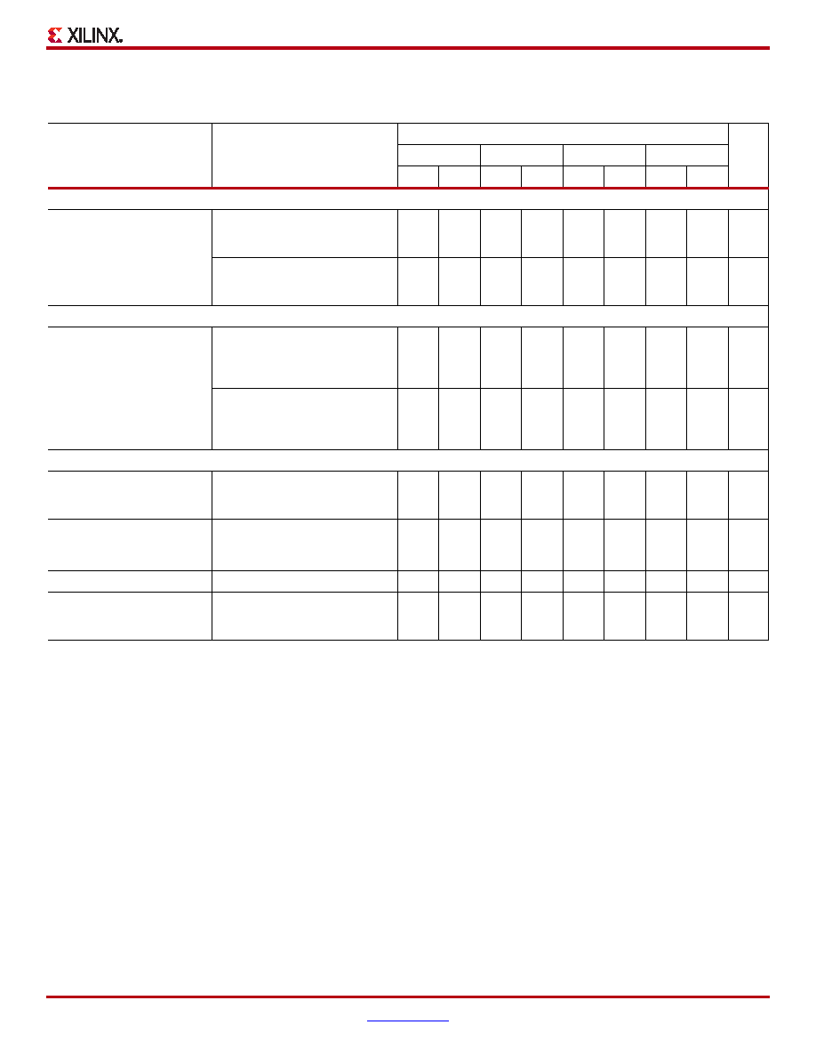
DCM Switching Characteristics
Table 53: Operating Frequency Ranges and Conditions for the Delay-Locked Loop (DLL)(1)
Symbol
Description
Speed Grade
Units
-3
-3N
-2
-1L
MinMax
Min
Max
MinMax
Input Frequency Ranges
CLKIN_FREQ_DLL
Frequency of the CLKIN clock
input when the CLKDV output is
not used.
5(2)
280(3)
5(2)
280(3)
5(2)
250(3)
5(2)
175(3)
MHz
Frequency of the CLKIN clock
input when using the CLKDV
output.
5(2)
280(3)
5(2)
280(3)
5(2)
250(3)
5(2)
133(3)
MHz
Input Pulse Requirements
CLKIN_PULSE
CLKIN pulse width as a
percentage of the CLKIN period
for
CLKIN_FREQ_DLL < 150 MHz
40
60
40
60
40
60
40
60
%
CLKIN pulse width as a
percentage of the CLKIN period
for
CLKIN_FREQ_DLL > 150 MHz
45
55
45
55
45
55
45
55
%
Input Clock Jitter Tolerance and Delay Path Variation(4)
CLKIN_CYC_JITT_DLL_LF
Cycle-to-cycle jitter at the CLKIN
input for
CLKIN_FREQ_DLL < 150 MHz
–
±300
–
±300
–
±300
–
±300
ps
CLKIN_CYC_JITT_DLL_HF
Cycle-to-cycle jitter at the CLKIN
input for
CLKIN_FREQ_DLL > 150 MHz.
–
±150
–
±150
–
±150
–
±150
ps
CLKIN_PER_JITT_DLL
Period jitter at the CLKIN input.
–
±1
–
±1
–
±1
–
±1
ns
CLKFB_DELAY_VAR_EXT
Allowable variation of the off-chip
feedback delay from the DCM
output to the CLKFB input.
–±1–
±1
–
±1
–
±1
ns
Notes:
1.
DLL specifications apply when using any of the DLL outputs: CLK0, CLK90, CLK180, CLK270, CLK2X, CLK2X180, or CLKDV.
2.
When operating independently of the DLL, the DFS supports lower CLKIN_FREQ_DLL frequencies. See Table 55.
3.
The CLKIN_DIVIDE_BY_2 attribute increases the effective input frequency range. When set to TRUE, the input clock frequency is divided by two as
it enters the DCM. Input clock frequencies for the clock buffer being used can be increased up to the FMAX (see Table 48 and Table 49 for BUFG and
BUFIO2 limits). When used with CLK_FEEDBACK=2X, the input clock frequency matches the frequency for CLK2X, and is limited to
CLKOUT_FREQ_2X.
4.
CLKIN_FREQ_DLL input jitter beyond these limits can cause the DCM to lose LOCK, indicated by the LOCKED output deasserting. The user must
then reset the DCM.
5.
When using both DCMs in a CMT, both DCMs must be LOCKED.
相关PDF资料 |
PDF描述 |
|---|---|
| XC6SLX45T-2FGG484I | IC FPGA SPARTAN 6 43K 484FGGBGA |
| 25LC080D-E/ST | IC SRL EEPROM 1KX8 2.5V 8-TSSOP |
| 25LC080C-E/MS | IC SRL EEPROM 1KX8 2.5V 8-MSOP |
| XC6SLX45T-N3CSG484I | IC FPGA SPARTAN-6 484CSBGA |
| 25AA320AXT-I/ST | IC EEPROM 32KBIT 10MHZ 8TSSOP |
相关代理商/技术参数 |
参数描述 |
|---|---|
| XC6SLX45T-2FGG484C | 功能描述:IC FPGA SPARTAN 6 43K 484FGGBGA RoHS:是 类别:集成电路 (IC) >> 嵌入式 - FPGA(现场可编程门阵列) 系列:Spartan® 6 LXT 标准包装:60 系列:XP LAB/CLB数:- 逻辑元件/单元数:10000 RAM 位总计:221184 输入/输出数:244 门数:- 电源电压:1.71 V ~ 3.465 V 安装类型:表面贴装 工作温度:0°C ~ 85°C 封装/外壳:388-BBGA 供应商设备封装:388-FPBGA(23x23) 其它名称:220-1241 |
| XC6SLX45T-2FGG484CES9982 | 制造商:Xilinx 功能描述: |
| XC6SLX45T-2FGG484I | 功能描述:IC FPGA SPARTAN 6 43K 484FGGBGA RoHS:是 类别:集成电路 (IC) >> 嵌入式 - FPGA(现场可编程门阵列) 系列:Spartan® 6 LXT 标准包装:40 系列:Spartan® 6 LX LAB/CLB数:3411 逻辑元件/单元数:43661 RAM 位总计:2138112 输入/输出数:358 门数:- 电源电压:1.14 V ~ 1.26 V 安装类型:表面贴装 工作温度:-40°C ~ 100°C 封装/外壳:676-BGA 供应商设备封装:676-FBGA(27x27) |
| XC6SLX45T-2FGG676C | 制造商:Xilinx 功能描述: |
| XC6SLX45T-2FGG676I | 制造商:Xilinx 功能描述: |
发布紧急采购,3分钟左右您将得到回复。