参数资料
| 型号: | XCV300E-8FG456C |
| 厂商: | Xilinx Inc |
| 文件页数: | 162/233页 |
| 文件大小: | 0K |
| 描述: | IC FPGA 1.8V C-TEMP 456-FBGA |
| 产品变化通告: | FPGA Family Discontinuation 18/Apr/2011 |
| 标准包装: | 1 |
| 系列: | Virtex®-E |
| LAB/CLB数: | 1536 |
| 逻辑元件/单元数: | 6912 |
| RAM 位总计: | 131072 |
| 输入/输出数: | 312 |
| 门数: | 411955 |
| 电源电压: | 1.71 V ~ 1.89 V |
| 安装类型: | 表面贴装 |
| 工作温度: | 0°C ~ 85°C |
| 封装/外壳: | 456-BBGA |
| 供应商设备封装: | 456-FBGA |
第1页第2页第3页第4页第5页第6页第7页第8页第9页第10页第11页第12页第13页第14页第15页第16页第17页第18页第19页第20页第21页第22页第23页第24页第25页第26页第27页第28页第29页第30页第31页第32页第33页第34页第35页第36页第37页第38页第39页第40页第41页第42页第43页第44页第45页第46页第47页第48页第49页第50页第51页第52页第53页第54页第55页第56页第57页第58页第59页第60页第61页第62页第63页第64页第65页第66页第67页第68页第69页第70页第71页第72页第73页第74页第75页第76页第77页第78页第79页第80页第81页第82页第83页第84页第85页第86页第87页第88页第89页第90页第91页第92页第93页第94页第95页第96页第97页第98页第99页第100页第101页第102页第103页第104页第105页第106页第107页第108页第109页第110页第111页第112页第113页第114页第115页第116页第117页第118页第119页第120页第121页第122页第123页第124页第125页第126页第127页第128页第129页第130页第131页第132页第133页第134页第135页第136页第137页第138页第139页第140页第141页第142页第143页第144页第145页第146页第147页第148页第149页第150页第151页第152页第153页第154页第155页第156页第157页第158页第159页第160页第161页当前第162页第163页第164页第165页第166页第167页第168页第169页第170页第171页第172页第173页第174页第175页第176页第177页第178页第179页第180页第181页第182页第183页第184页第185页第186页第187页第188页第189页第190页第191页第192页第193页第194页第195页第196页第197页第198页第199页第200页第201页第202页第203页第204页第205页第206页第207页第208页第209页第210页第211页第212页第213页第214页第215页第216页第217页第218页第219页第220页第221页第222页第223页第224页第225页第226页第227页第228页第229页第230页第231页第232页第233页
Virtex-E 1.8 V Field Programmable Gate Arrays
R
Module 2 of 4
DS022-2 (v3.0) March 21, 2014
28
Production Product Specification
— OBSOLETE — OBSOLETE — OBSOLETE — OBSOLETE —
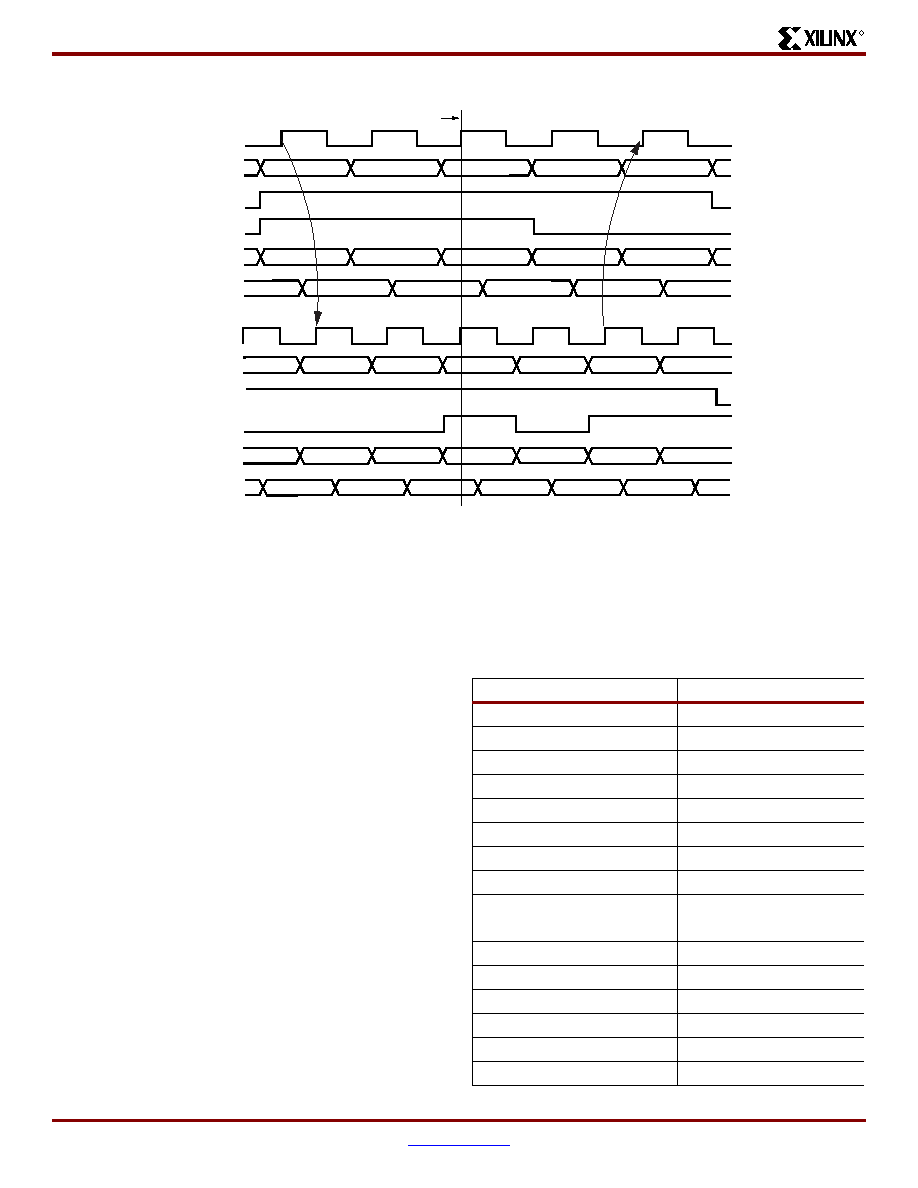
At the third rising edge of CLKA, the TBCCS parameter is
violated with two writes to memory location 0x0F. The DOA
and DOB buses reflect the contents of the DIA and DIB
buses, but the stored value at 0x0F is invalid.
At the fourth rising edge of CLKA, a read operation is per-
formed at memory location 0x0F and invalid data is present
on the DOA bus. Port B also executes a read operation to
memory location 0x0F and also reads invalid data.
At the fifth rising edge of CLKA a read operation is per-
formed that does not violate the TBCCS parameter to the
previous write of 0x7E by Port B. THe DOA bus reflects the
recently written value by Port B.
Initialization
The block SelectRAM+ memory can initialize during the
device configuration sequence. The 16 initialization properties
of 64 hex values each (a total of 4096 bits) set the initialization
of each RAM. These properties appear in Table 17. Any initial-
ization properties not explicitly set configure as zeros. Partial
initialization strings pad with zeros. Initialization strings
greater than 64 hex values generate an error. The RAMs can
be simulated with the initialization values using generics in
VHDL simulators and parameters in Verilog simulators.
Initialization in VHDL and Synopsys
The block SelectRAM+ structures can be initialized in VHDL
for both simulation and synthesis for inclusion in the EDIF
output file. The simulation of the VHDL code uses a generic
to pass the initialization. Synopsys FPGA compiler does not
presently support generics. The initialization values instead
attach as attributes to the RAM by a built-in Synopsys
dc_script. The translate_off statement stops synthesis
translation of the generic statements. The following code
illustrates a module that employs these techniques.
Figure 34: Timing Diagram for a True Dual-port Read/Write Block SelectRAM+ Memory
ds022_035_121399
CLK_A
PORT
A
PORT
B
ADDR_A
00
7E
0F
00
7E
1A
0F
7E
AAAA
9999
AAAA
0000
1111
2222
AAAA
9999
AAAA
UNKNOWN
EN_A
WE_A
DI_A
DO_A
1111
2222
FFFF
BBBB
1111
AAAA
MEM (00)
9999
2222
FFFF
BBBB
UNKNOWN
CLK_B
ADDR_B
EN_B
WE_B
DI_B
DO_B
TBCCS
VIOLATION
TBCCS
Table 17: RAM Initialization Properties
Property
Memory Cells
INIT_00
255 to 0
INIT_01
511 to 256
INIT_02
767 to 512
INIT_03
1023 to 768
INIT_04
1279 to 1024
INIT_05
1535 to 1280
INIT_06
1791 to 2047
INIT_07
2047 to 1792
INIT_08
2303 to 2048
INIT_09
2559 to 2304
INIT_0a
2815 to 2560
INIT_0b
3071 to 2816
INIT_0c
3327 to 3072
INIT_0d
3583 to 3328
INIT_0e
3839 to 3584
INIT_0f
4095 to 3840
相关PDF资料 |
PDF描述 |
|---|---|
| XCV300E-7FG456I | IC FPGA 1.8V I-TEMP 456-FBGA |
| XC2V2000-4FGG676C | IC VIRTEX-II FPGA 2M 676-FBGA |
| XC5VLX50-1FFG1153C | IC FPGA VIRTEX-5 50K 1153FBGA |
| XC2V1500-4FG676I | IC FPGA VIRTEX-II 676FGBGA |
| 4-1393561-8 | CONN D-SUB CABLE BUSHING 9-37POS |
相关代理商/技术参数 |
参数描述 |
|---|---|
| XCV300E-8FG456I | 制造商:XILINX 制造商全称:XILINX 功能描述:Virtex-E 1.8 V Field Programmable Gate Arrays |
| XCV300E-8HQ204C | 制造商:XILINX 制造商全称:XILINX 功能描述:Virte -E 1.8 V Field Programmable Gate Arrays |
| XCV300E-8HQ204I | 制造商:XILINX 制造商全称:XILINX 功能描述:Virte -E 1.8 V Field Programmable Gate Arrays |
| XCV300E-8HQ240C | 制造商:XILINX 制造商全称:XILINX 功能描述:Virtex-E 1.8 V Field Programmable Gate Arrays |
| XCV300E-8HQ240I | 制造商:XILINX 制造商全称:XILINX 功能描述:Virtex⑩-E 1.8 V Field Programmable Gate Arrays |
发布紧急采购,3分钟左右您将得到回复。