参数资料
| 型号: | XCV812E-6FG900C |
| 厂商: | Xilinx Inc |
| 文件页数: | 43/118页 |
| 文件大小: | 0K |
| 描述: | IC FPGA 1.8V C-TEMP 900-FBGA |
| 产品变化通告: | FPGA Family Discontinuation 18/Apr/2011 |
| 标准包装: | 1 |
| 系列: | Virtex®-E EM |
| LAB/CLB数: | 4704 |
| 逻辑元件/单元数: | 21168 |
| RAM 位总计: | 1146880 |
| 输入/输出数: | 556 |
| 门数: | 254016 |
| 电源电压: | 1.71 V ~ 1.89 V |
| 安装类型: | 表面贴装 |
| 工作温度: | 0°C ~ 85°C |
| 封装/外壳: | 900-BBGA |
| 供应商设备封装: | 900-FBGA |
第1页第2页第3页第4页第5页第6页第7页第8页第9页第10页第11页第12页第13页第14页第15页第16页第17页第18页第19页第20页第21页第22页第23页第24页第25页第26页第27页第28页第29页第30页第31页第32页第33页第34页第35页第36页第37页第38页第39页第40页第41页第42页当前第43页第44页第45页第46页第47页第48页第49页第50页第51页第52页第53页第54页第55页第56页第57页第58页第59页第60页第61页第62页第63页第64页第65页第66页第67页第68页第69页第70页第71页第72页第73页第74页第75页第76页第77页第78页第79页第80页第81页第82页第83页第84页第85页第86页第87页第88页第89页第90页第91页第92页第93页第94页第95页第96页第97页第98页第99页第100页第101页第102页第103页第104页第105页第106页第107页第108页第109页第110页第111页第112页第113页第114页第115页第116页第117页第118页
Virtex-E 1.8 V Extended Memory Field Programmable Gate Arrays
Module 2 of 4
DS025-2 (v3.0) March 21, 2014
26
R
— OBSOLETE — OBSOLETE — OBSOLETE — OBSOLETE —
Port Signals
Each block SelectRAM+ port operates independently of the
others while accessing the same set of 4096 memory cells.
Table 15 describes the depth and width aspect ratios for the
block SelectRAM+ memory.
Clock—CLK[A|B]
Each port is fully synchronous with independent clock pins.
All port input pins have setup time referenced to the port
CLK pin. The data output bus has a clock-to-out time refer-
enced to the CLK pin.
Enable—EN[A|B]
The enable pin affects the read, write and reset functionality
of the port. Ports with an inactive enable pin keep the output
pins in the previous state and do not write data to the mem-
ory cells.
Write Enable—WE[A|B]
Activating the write enable pin allows the port to write to the
memory cells. When active, the contents of the data input
bus are written to the RAM at the address pointed to by the
address bus, and the new data also reflects on the data out
bus. When inactive, a read operation occurs and the con-
tents of the memory cells referenced by the address bus
reflect on the data out bus.
Reset—RST[A|B]
The reset pin forces the data output bus latches to zero syn-
chronously. This does not affect the memory cells of the
RAM and does not disturb a write operation on the other
port.
Address Bus—ADDR[A|B]<#:0>
The address bus selects the memory cells for read or write.
The width of the port determines the required width of this
bus as shown in Table 15.
Data In Bus—DI[A|B]<#:0>
The data in bus provides the new data value to be written
into the RAM. This bus and the port have the same width, as
shown in Table 15.
Data Output Bus—DO[A|B]<#:0>
The data out bus reflects the contents of the memory cells
referenced by the address bus at the last active clock edge.
During a write operation, the data out bus reflects the data
in bus. The width of this bus equals the width of the port.
The allowed widths appear in Table 15.
Inverting Control Pins
The four control pins (CLK, EN, WE and RST) for each port
have independent inversion control as a configuration option.
Address Mapping
Each port accesses the same set of 4096 memory cells
using an addressing scheme dependent on the width of the
port. The physical RAM location addressed for a particular
width are described in the following formula (of interest only
when the two ports use different aspect ratios).
Start = ((ADDRport +1) * Widthport) –1
End = ADDRport * Widthport
Table 16 shows low order address mapping for each port
width.
Creating Larger RAM Structures
The block SelectRAM+ columns have specialized routing to
allow cascading blocks together with minimal routing
delays. This achieves wider or deeper RAM structures with
a smaller timing penalty than when using normal routing
channels.
Location Constraints
Block SelectRAM+ instances can have LOC properties
attached to them to constrain the placement. The block
SelectRAM+ placement locations are separate from the
CLB location naming convention, allowing the LOC proper-
ties to transfer easily from array to array.
The LOC properties use the following form.
LOC = RAMB4_R#C#
RAMB4_R0C0 is the upper left RAMB4 location on the
device.
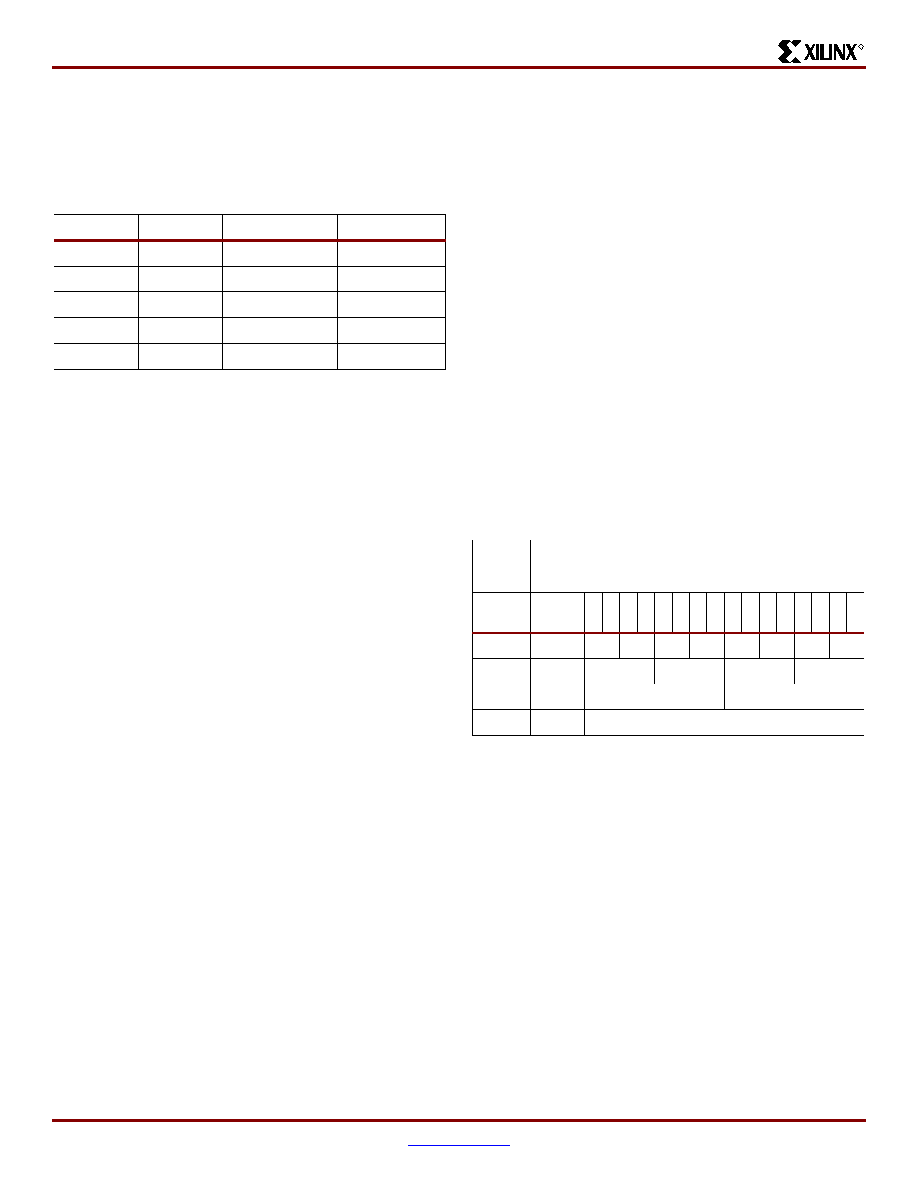
Table 15:
Block SelectRAM+ Port Aspect Ratios
Width
Depth
ADDR Bus
Data Bus
1
4096
ADDR<11:0>
DATA<0>
2
2048
ADDR<10:0>
DATA<1:0>
4
1024
ADDR<9:0>
DATA<3:0>
8
512
ADDR<8:0>
DATA<7:0>
16
256
ADDR<7:0>
DATA<15:0>
Table 16:
Port Address Mapping
Port
Width
Port
Addresses
1
4095...
1
5
1
4
1
3
1
2
1
0
9
0
8
0
7
0
6
0
5
0
4
0
3
0
2
0
1
0
2
2047...
07
06
05
04
03
02
01
00
4
1023...
03
02
01
00
8
511...
01
00
16
255...
00
相关PDF资料 |
PDF描述 |
|---|---|
| RCB106DHAR-S621 | EDGECARD 212POS DIP R/A .050 SLD |
| XC6VLX240T-1FFG1759C | IC FPGA VIRTEX 6 241K 1759FFGBGA |
| ACC65DRXN | CONN EDGECARD 130PS .100 DIP SLD |
| RMC65DRYI-S734 | CONN EDGECARD 130PS DIP .100 SLD |
| XC4VSX55-10FF1148I | IC FPGA VIRTEX-4SX 1148FFBGA |
相关代理商/技术参数 |
参数描述 |
|---|---|
| XCV812E-6FG900I | 制造商:XILINX 制造商全称:XILINX 功能描述:Virtex-E 1.8 V Extended Memory Field Programmable Gate Arrays |
| XCV812E-7BG404C | 制造商:XILINX 制造商全称:XILINX 功能描述:Virtex-E 1.8 V Extended Memory Field Programmable Gate Arrays |
| XCV812E-7BG404I | 制造商:XILINX 制造商全称:XILINX 功能描述:Virtex-E 1.8 V Extended Memory Field Programmable Gate Arrays |
| XCV812E-7BG556C | 制造商:XILINX 制造商全称:XILINX 功能描述:Virtex-E 1.8 V Extended Memory Field Programmable Gate Arrays |
| XCV812E-7BG556I | 制造商:XILINX 制造商全称:XILINX 功能描述:Virtex-E 1.8 V Extended Memory Field Programmable Gate Arrays |
发布紧急采购,3分钟左右您将得到回复。