- 您现在的位置:买卖IC网 > PDF目录10561 > XRT91L32IQ-F (Exar Corporation)IC TXRX SONET/SDH 8BIT 100QFP PDF资料下载
参数资料
| 型号: | XRT91L32IQ-F |
| 厂商: | Exar Corporation |
| 文件页数: | 19/37页 |
| 文件大小: | 0K |
| 描述: | IC TXRX SONET/SDH 8BIT 100QFP |
| 标准包装: | 20 |
| 类型: | 收发器 |
| 规程: | SONET/SDH |
| 电源电压: | 3.3V |
| 安装类型: | 表面贴装 |
| 封装/外壳: | 100-BQFP |
| 供应商设备封装: | 100-QFP(14x20) |
| 包装: | 托盘 |
| 其它名称: | 1016-1489 XRT91L32IQ-F-ND |
第1页第2页第3页第4页第5页第6页第7页第8页第9页第10页第11页第12页第13页第14页第15页第16页第17页第18页当前第19页第20页第21页第22页第23页第24页第25页第26页第27页第28页第29页第30页第31页第32页第33页第34页第35页第36页第37页
XRT91L32
xr
STS-12/STM-4 OR STS-3/STM-1 SONET/SDH TRANSCEIVER
REV. 1.0.3
24
Jitter specification is defined using a 12kHz to 1.3/5MHz LP-HP single-pole filter.
1These reference clock jitter limits are required for the outputs to meet SONET system level jitter requirements (<10 mUI
rms).
2Required to meet SONET output frequency stability requirements.
3.5
Loop Timing and Clock Control
Two types of loop timing are possible in the XRT91L32.
In the internal loop timing mode, loop timing is controlled by the LOOPTIME pin. This mode is selected by
asserting the LOOPTIME signal to a high level. When the loop timing mode is activated, the CMU synthesized
hi-speed reference clock input to the Retimer is replaced with the hi-speed internally recovered receive clock
coming from the CDR. Under this condition both the transmit and receive sections are synchronized to the
internally recovered receive clock. Loop time mode directly locks the Retimer to the recovered receive clock.
In external loop timing mode, the XRT91L32 allows the user the flexibility of using an externally recovered
receive clock for retiming the high speed serial data. First, the CDRDIS input pin should be set high. By doing
so, the internal CDR is disabled and bypassed and the XRT91L32 will sample the incoming high speed serial
data on RXIP/N with the externally recovered receive clock connected to the XRXCLKIP/N inputs. In this state,
the receive clock de-jittering and recovery is done externally and fed thru XRXCLKIP/N and the XRT91L32 will
sample RXIP/N on the rising edge of XRXCLKIP/N. Secondly, the LOOPTIME pin must also be set high in
order to select the externally recovered receive clock on XRXCLKIP/N as the reference clock source for the
transmit serial data output stream TXOP/N.
Table 13 provides configuration for selecting the loop timing and clock recovery modes. The use of the on-chip
CDR or an external recovered clock in loop timing applications is shown in Figure 14.
ECLKJIT
STS-12/STM-4 Electrical Clock output jitter (rms) with 77.76 MHz reference
4
mUIrms
OCLKFREQ
Frequency output
620
624
MHz
OCYCDUTY
Clock output duty cycle (’1010’ data pattern)
45
55
%
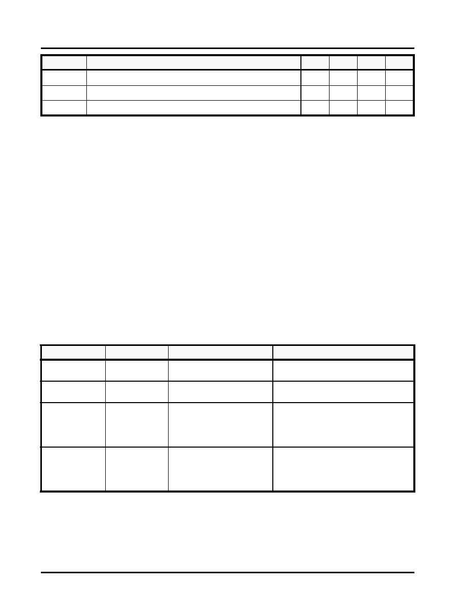
TABLE 13: LOOP TIMING AND CLOCK RECOVERY CONFIGURATIONS
CDRDIS
LOOPTIME
TRANSMIT CLOCK SOURCE
RECEIVE CLOCK SOURCE
0
Clock Multiplier Unit
CDR Enabled.
Clock and Data recovery by internal CDR
0
1
Internal CDR
CDR Enabled.
Clock and Data recovery by internal CDR
1
0
Clock Multiplier Unit
CDR Disabled.
Externally recovered Receive Clock from
XRXCLKIP/N
622.08/155.52 Mbps data on RXIP/N sampled at
rising edge of XRXCLKIP/N
1
External CDR thru XRXCLKIP/N
CDR Disabled.
Externally recovered Receive Clock from
XRXCLKIP/N
622.08/155.52 Mbps data on RXIP/N sampled at
rising edge of XRXCLKIP/N
NAME
PARAMETER
MIN
TYP
MAX
UNITS
相关PDF资料 |
PDF描述 |
|---|---|
| XRT91L30IQ-F | IC TXRX SONET/SDH 8BIT 64QFP |
| VI-BTF-MX-F1 | CONVERTER MOD DC/DC 72V 75W |
| XRT75VL00DIV-F | IC LIU E3/DS3/STS-1 1CH 52TQFP |
| VI-BTF-MW | CONVERTER MOD DC/DC 72V 100W |
| VI-BT4-MX-F3 | CONVERTER MOD DC/DC 48V 75W |
相关代理商/技术参数 |
参数描述 |
|---|---|
| XRT91L32IQTR | 功能描述:LIN 收发器 PHY Transceiver RoHS:否 制造商:NXP Semiconductors 工作电源电压: 电源电流: 最大工作温度: 封装 / 箱体:SO-8 |
| XRT91L32IQTR-F | 功能描述:LIN 收发器 PHY Transceiver RoHS:否 制造商:NXP Semiconductors 工作电源电压: 电源电流: 最大工作温度: 封装 / 箱体:SO-8 |
| XRT91L33 | 制造商:EXAR 制造商全称:EXAR 功能描述:STS-12/STS-3 MULTIRATE CLOCK AND DATA RECOVERY UNIT |
| XRT91L33AIG-F | 制造商:Exar Corporation 功能描述:CDR 155.52Mbps/622.08Mbps SONET/SDH 20-Pin TSSOP |
| XRT91L33ES | 功能描述:界面开发工具 Eval System for XRT91L33 Series RoHS:否 制造商:Bourns 产品:Evaluation Boards 类型:RS-485 工具用于评估:ADM3485E 接口类型:RS-485 工作电源电压:3.3 V |
发布紧急采购,3分钟左右您将得到回复。