- 您现在的位置:买卖IC网 > PDF目录13598 > ZL2106ALCFT (Intersil)IC REG BUCK SYNC ADJ 6A 36QFN PDF资料下载
参数资料
| 型号: | ZL2106ALCFT |
| 厂商: | Intersil |
| 文件页数: | 19/29页 |
| 文件大小: | 0K |
| 描述: | IC REG BUCK SYNC ADJ 6A 36QFN |
| 标准包装: | 4,000 |
| 类型: | 降压(降压) |
| 输出类型: | 可调式 |
| 输出数: | 1 |
| 输出电压: | 0.54 V ~ 5.5 V |
| 输入电压: | 4.5 V ~ 14 V |
| PWM 型: | 电压模式 |
| 频率 - 开关: | 200kHz ~ 1MHz |
| 电流 - 输出: | 6A |
| 同步整流器: | 是 |
| 工作温度: | -40°C ~ 85°C |
| 安装类型: | 表面贴装 |
| 封装/外壳: | 36-VFQFN 裸露焊盘 |
| 包装: | 带卷 (TR) |
| 供应商设备封装: | 36-QFN(6x6) |
第1页第2页第3页第4页第5页第6页第7页第8页第9页第10页第11页第12页第13页第14页第15页第16页第17页第18页当前第19页第20页第21页第22页第23页第24页第25页第26页第27页第28页第29页
�� �
�
�ZL2106�
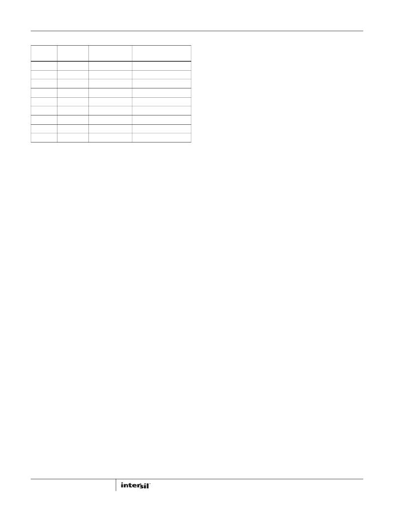
�TABLE� 12.� RESISTOR� SETTING� FOR� LOOP� COMPENSATION� (Continued)�
�2.� Continue� operating� for� a� given� delay� period,� followed� by�
�G� (dB)�
�33�
�33�
�33�
�33�
�33�
�33�
�33�
�33�
�33�
�Q�
�0.150�
�0.150�
�0.300�
�0.300�
�0.300�
�0.300�
�0.600�
�0.600�
�0.600�
�fsw/fn�
�69.147�
�41.577�
�115.000�
�69.147�
�41.577�
�25.000�
�69.147�
�41.577�
�25.000�
�FC�
�(k)�
�82.5�
�90.9�
�100.0�
�110.0�
�121.0�
�133.0�
�147.0�
�162.0�
�178.0�
�shutdown� if� the� fault� still� exists.� The� device� will� remain� in�
�shutdown� until� instructed� to� restart.�
�3.� Initiate� an� immediate� shutdown� until� the� fault� has� been�
�cleared.� The� user� can� select� a� specific� number� of� retry�
�attempts.�
�The� default� response� from� a� UVLO� fault� is� an� immediate� shutdown�
�of� the� device.� Please� refer� to� Application� Note� AN2033� for� details� on�
�how� to� configure� the� UVLO� threshold� or� to� select� specific� UVLO� fault�
�response� options� via� the� I� 2� C/SMBus� interface.�
�Output� Overvoltage� Protection�
�The� ZL2106� offers� an� internal� output� overvoltage� protection�
�circuit� that� can� be� used� to� protect� sensitive� load� circuitry� from�
�In� the� ZL2106,� the� compensation� zeros� are� set� by� configuring� the�
�FC� pin� or� via� the� I� 2� C/SMBus� interface� once� the� user� has�
�calculated� the� required� settings.� This� method� eliminates� the�
�inaccuracies� due� to� the� component� tolerances� associated� with�
�using� external� resistors� and� capacitors� required� with� traditional�
�analog� controllers.�
�The� loop� compensation� coefficients� can� also� be� set� via� the�
�I� 2� C/SMBus� interface.� Please� refer� to� Application� Note� AN2033�
�for� further� details.� Also� refer� to� Application� Note� AN2035� for�
�further� technical� details� on� setting� loop� compensation.�
�Driver� Dead-time� Control�
�The� ZL2106� utilizes� a� predetermined� fixed� dead-time� applied�
�between� the� gate� drive� signals� for� the� top� and� bottom� MOSFETs.�
�In� a� synchronous� buck� converter,� the� MOSFET� drive� circuitry� must�
�be� operated� such� that� the� top� and� bottom� MOSFETs� are� never� in�
�the� conducting� state� at� the� same� time.� This� is� because�
�potentially� damaging� currents� flow� in� the� circuit� if� both� MOSFETs�
�are� on� simultaneously� for� periods� of� time� exceeding� a� few�
�nanoseconds.� Conversely,� long� periods� of� time� in� which� both�
�MOSFETs� are� off� reduces� overall� circuit� efficiency� by� allowing�
�current� to� flow� in� their� parasitic� body� diodes.�
�Therefore,� it� is� advantageous� to� minimize� the� dead-time� to�
�provide� peak� optimal� efficiency� without� compromising� system�
�reliability.� The� ZL2106� has� optimized� the� dead-time� for� the�
�integrated� MOSFETs� to� maximizing� efficiency.�
�Power� Management� Functional�
�Description�
�Input� Undervoltage� Lockout�
�The� input� undervoltage� lockout� (UVLO)� prevents� the� ZL2106� from�
�operating� when� the� input� falls� below� a� preset� threshold,�
�indicating� the� input� supply� is� out� of� its� specified� range.� The� UVLO�
�threshold� (V� UVLO� )� can� be� set� to� either� 4.5V� or� 10.8V� using� the� SS�
�pin� according� to� Table� 6.�
�The� UVLO� voltage� can� also� be� set� to� any� value� between� 2.85V�
�and� 16V� via� the� I� 2� C/SMBus� interface.�
�Once� an� input� undervoltage� fault� condition� occurs,� the� device�
�can� respond� in� a� number� of� ways� as� follows:�
�1.� Continue� operating� without� interruption.�
�19�
�being� subjected� to� a� voltage� higher� than� its� prescribed� limits.� A�
�hardware� comparator� is� used� to� compare� the� actual� output�
�voltage� (seen� at� the� VSEN� pin)� to� a� threshold� set� to� 15%� higher�
�than� the� target� output� voltage� (the� default� setting).� If� the� VSEN�
�voltage� exceeds� this� threshold,� the� PG� pin� will� de-assert� and� the�
�device� can� then� respond� in� a� number� of� ways� as� follows:�
�1.� Initiate� an� immediate� shutdown� until� the� fault� has� been�
�cleared.� The� user� can� select� a� specific� number� of� retry�
�attempts.�
�2.� Turn� off� the� high-side� MOSFET� and� turn� on� the� low-side�
�MOSFET.� The� low-side� MOSFET� remains� on� until� the� device�
�attempts� a� restart.�
�The� default� response� from� an� overvoltage� fault� is� to� immediately�
�shut� down.� For� continuous� overvoltage� protection� when� operating�
�from� an� external� clock,� the� only� allowed� response� is� an�
�immediate� shutdown.� Please� refer� to� Application� Note� AN2033�
�for� details� on� how� to� select� specific� overvoltage� fault� response�
�options� via� I� 2� C/SMBus.�
�Output� Pre-Bias� Protection�
�An� output� pre-bias� condition� exists� when� an� externally� applied�
�voltage� is� present� on� a� power� supply’s� output� before� the� power�
�supply’s� control� IC� is� enabled.� Certain� applications� require� that�
�the� converter� not� be� allowed� to� sink� current� during� start� up� if� a�
�pre-bias� condition� exists� at� the� output.� The� ZL2106� provides�
�pre-bias� protection� by� sampling� the� output� voltage� prior� to�
�initiating� an� output� ramp.�
�If� a� pre-bias� voltage� lower� than� the� target� voltage� exists� after� the�
�pre-configured� delay� period� has� expired,� the� target� voltage� is� set�
�to� match� the� existing� pre-bias� voltage� and� both� drivers� are�
�enabled.� The� output� voltage� is� then� ramped� to� the� final�
�regulation� value� at� the� ramp� rate� set� by� the� SS� pin.�
�The� actual� time� the� output� will� take� to� ramp� from� the� pre-bias�
�voltage� to� the� target� voltage� will� vary� depending� on� the� pre-bias�
�voltage� but� the� total� time� elapsed� from� when� the� delay� period�
�expires� and� when� the� output� reaches� its� target� value� will� match�
�the� pre-configured� ramp� time� (see� Figure� 18).�
�If� a� pre-bias� voltage� higher� than� the� target� voltage� exists� after� the�
�pre-configured� delay� period� has� expired,� the� target� voltage� is� set�
�to� match� the� existing� pre-bias� voltage� and� both� drivers� are�
�enabled� with� a� PWM� duty� cycle� that� would� ideally� create� the� pre-�
�bias� voltage.�
�FN6852.6�
�February� 20,� 2013�
�相关PDF资料 |
PDF描述 |
|---|---|
| ISL8033IRZ-T | IC REG BUCK SYNC ADJ 3A DL 24QFN |
| 16RX30680MT810X16 | CAP ALUM 680UF 16V 20% RADIAL |
| UPM1J100MDD | CAP ALUM 10UF 63V 20% RADIAL |
| RBC61DCMN | CONN EDGECARD 122POS .100 WW |
| GBA49DRMD | CONN EDGECARD 98POS .125 SQ WW |
相关代理商/技术参数 |
参数描述 |
|---|---|
| ZL2106ALCFTK | 功能描述:IC REG BUCK SYNC ADJ 6A 36QFN RoHS:是 类别:集成电路 (IC) >> PMIC - 稳压器 - DC DC 开关稳压器 系列:- 产品培训模块:Lead (SnPb) Finish for COTS Obsolescence Mitigation Program 标准包装:2,500 系列:- 类型:降压(降压) 输出类型:两者兼有 输出数:1 输出电压:5V,1 V ~ 10 V 输入电压:3.5 V ~ 28 V PWM 型:电流模式 频率 - 开关:220kHz ~ 1MHz 电流 - 输出:600mA 同步整流器:无 工作温度:-40°C ~ 125°C 安装类型:表面贴装 封装/外壳:16-SSOP(0.154",3.90mm 宽) 包装:带卷 (TR) 供应商设备封装:16-QSOP |
| ZL2106ALCFTR5520 | 制造商:Intersil Corporation 功能描述:6A DIGITAL DC-DC CONVERTER W/ DDC - TR4K - Tape and Reel |
| ZL2106ALCN | 功能描述:IC REG BUCK SYNC ADJ 6A 36QFN RoHS:是 类别:集成电路 (IC) >> PMIC - 稳压器 - DC DC 开关稳压器 系列:- 产品培训模块:Lead (SnPb) Finish for COTS Obsolescence Mitigation Program 标准包装:1 系列:- 类型:降压(降压) 输出类型:固定 输出数:1 输出电压:3.3V 输入电压:4.5 V ~ 24 V PWM 型:- 频率 - 开关:- 电流 - 输出:125mA 同步整流器:无 工作温度:-40°C ~ 85°C 安装类型:表面贴装 封装/外壳:SOT-23-6 包装:Digi-Reel® 供应商设备封装:SOT-6 其它名称:MAX1836EUT33#TG16DKR |
| ZL2106ALCNT | 功能描述:IC REG BUCK SYNC ADJ 6A 36QFN RoHS:是 类别:集成电路 (IC) >> PMIC - 稳压器 - DC DC 开关稳压器 系列:- 产品培训模块:Lead (SnPb) Finish for COTS Obsolescence Mitigation Program 标准包装:1 系列:- 类型:降压(降压) 输出类型:固定 输出数:1 输出电压:3.3V 输入电压:4.5 V ~ 24 V PWM 型:- 频率 - 开关:- 电流 - 输出:125mA 同步整流器:无 工作温度:-40°C ~ 85°C 安装类型:表面贴装 封装/外壳:SOT-23-6 包装:Digi-Reel® 供应商设备封装:SOT-6 其它名称:MAX1836EUT33#TG16DKR |
| ZL2106ALCNTK | 功能描述:IC REG BUCK SYNC ADJ 6A 36QFN RoHS:是 类别:集成电路 (IC) >> PMIC - 稳压器 - DC DC 开关稳压器 系列:- 产品培训模块:Lead (SnPb) Finish for COTS Obsolescence Mitigation Program 标准包装:1 系列:- 类型:降压(降压) 输出类型:固定 输出数:1 输出电压:3.3V 输入电压:4.5 V ~ 24 V PWM 型:- 频率 - 开关:- 电流 - 输出:125mA 同步整流器:无 工作温度:-40°C ~ 85°C 安装类型:表面贴装 封装/外壳:SOT-23-6 包装:Digi-Reel® 供应商设备封装:SOT-6 其它名称:MAX1836EUT33#TG16DKR |
发布紧急采购,3分钟左右您将得到回复。