- 您现在的位置:买卖IC网 > Datasheet目录540 > ZXMN20B28KTC (Diodes Inc)MOSFET N-CH 200V 1.5A DPAK Datasheet资料下载
参数资料
| 型号: | ZXMN20B28KTC |
| 厂商: | Diodes Inc |
| 文件页数: | 2/8页 |
| 文件大小: | 0K |
| 描述: | MOSFET N-CH 200V 1.5A DPAK |
| 标准包装: | 1 |
| FET 型: | MOSFET N 通道,金属氧化物 |
| FET 特点: | 逻辑电平门 |
| 漏极至源极电压(Vdss): | 200V |
| 电流 - 连续漏极(Id) @ 25° C: | 1.5A |
| 开态Rds(最大)@ Id, Vgs @ 25° C: | 750 毫欧 @ 2.75A,10V |
| Id 时的 Vgs(th)(最大): | 2.5V @ 250µA |
| 闸电荷(Qg) @ Vgs: | 8.1nC @ 5V |
| 输入电容 (Ciss) @ Vds: | 358pF @ 25V |
| 功率 - 最大: | 2.2W |
| 安装类型: | 表面贴装 |
| 封装/外壳: | TO-252-3,DPak(2 引线+接片),SC-63 |
| 供应商设备封装: | TO-252-3 |
| 包装: | 标准包装 |
| 其它名称: | ZXMN20B28KTCDKR |
�� �
�
�A� Product� Line� of�
�Diodes� Incorporated�
�ZXMN20B28K�
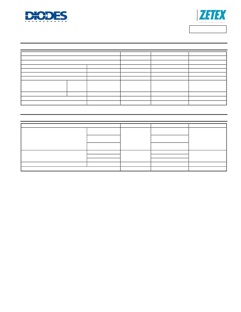
�Maximum� Ratings�
�@T� A� =� 25°C� unless� otherwise� specified�
�Drain-Source� voltage�
�Gate-Source� voltage�
�Characteristic�
�Symbol�
�V� DSS�
�V� GS�
�Value�
�200�
�±� 20�
�Unit�
�V�
�V�
�Single� Pulsed� Avalanche� Energy�
�Single� Pulsed� Avalanche� Current�
�Repetitive� Avalanche� Energy�
�Repetitive� Avalanche� Current�
�(Note� 7)�
�(Note� 7)�
�(Note� 4)�
�(Note� 4)�
�E� AS�
�I� AS�
�E� AR�
�I� AR�
�73�
�5.5�
�4.5�
�5.5�
�mJ�
�A�
�mJ�
�A�
�Continuous� Drain� current�
�V� GS� =� 10V�
�(Note� 3)�
�T� A� =� 70� °� C� (Note� 3)�
�I� D�
�2.3�
�1.8�
�A�
�(Note� 2)�
�1.5�
�Pulsed� Drain� current�
�V� GS� =� 10V�
�(Note� 4)�
�I� DM�
�17.3�
�A�
�Continuous� Source� current� (Body� diode)�
�Pulsed� Source� current� (Body� diode)�
�(Note� 2)�
�(Note� 4)�
�I� S�
�I� SM�
�5.7�
�17.3�
�A�
�A�
�Thermal� Characteristics�
�Characteristic�
�(Note� 2)�
�Symbol�
�Value�
�4.3�
�34.4�
�Unit�
�Power� dissipation�
�Linear� derating� factor�
�(Note� 3)�
�P� D�
�10.2�
�76.0�
�W�
�mW/� °� C�
�(Note� 6)�
�(Note� 2)�
�2.2�
�17.4�
�29.1�
�Thermal� Resistance,� Junction� to� Ambient�
�(Note� 3)�
�R� θ� JA�
�12.3�
�°� C/W�
�(Note� 6)�
�57.3�
�Thermal� Resistance,� Junction� to� Lead�
�Operating� and� storage� temperature� range�
�(Note� 5)�
�R� θ� JL�
�T� J� ,� T� STG�
�1.15�
�-55� to� 150�
�°� C/W�
�°� C�
�Notes:�
�2.� For� a� device� surface� mounted� on� 50mm� x� 50mm� x� 1.6mm� FR4� PCB� with� high� coverage� of� single� sided� 2oz� copper,� in� still� air� conditions;� the� device� is�
�measured� when� operating� in� a� steady-state� condition.�
�3.� Same� as� note� 2,� except� the� device� is� measured� at� t� ≤� 10� sec.�
�4.� Same� as� note� 2,� except� the� device� is� operating� in� a� repetitive� state� with� pulse� width� and� duty� cycle� limited� by� maximum� junction� temperature.�
�5.� Thermal� resistance� from� junction� to� solder-point� (at� the� end� of� the� drain� lead).�
�6.� For� a� device� surface� mounted� on� 25mm� x� 25mm� x� 1.6mm� FR4� PCB� with� the� high� coverage� single� sided� 1oz� copper,� in� still� air� conditions;� the� device� is�
�measured� when� operating� in� a� steady-state� condition.�
�7.� UIS� in� production� with� L� =� 4.83mH,� I� AS� =� 5.5A,� R� G� =� 25� ?� ,� V� DD� =� 100V,� starting� T� J� =� 25°C.�
�ZXMN20B28K�
�Document� Number� DS31984� Rev.� 2� -� 2�
�2� of� 8�
�www.diodes.com�
�October� 2009�
�?� Diodes� Incorporated�
�相关PDF资料 |
PDF描述 |
|---|---|
| ZXMN2A01E6TC | MOSFET N-CHAN 20V SOT23-6 |
| ZXMN2A01FTC | MOSFET N-CHAN 20V SOT23-3 |
| ZXMN2A02N8TA | MOSFET N-CH 20V 8.3A 8-SOIC |
| ZXMN2A02X8TC | MOSFET N-CH 20V 6.2A 8-MSOP |
| ZXMN2A03E6TC | MOSFET N-CHAN 20V SOT23-6 |
相关代理商/技术参数 |
参数描述 |
|---|---|
| ZXMN2A01 | 制造商:ZETEX 制造商全称:ZETEX 功能描述:20V N-CHANNEL ENHANCEMENT MODE MOSFET |
| ZXMN2A01E6 | 制造商:Diodes Incorporated 功能描述:MOSFET N SOT-23-6 |
| ZXMN2A01E6_06 | 制造商:ZETEX 制造商全称:ZETEX 功能描述:20V N-CHANNEL ENHANCEMENT MODE MOSFET |
| ZXMN2A01E6TA | 功能描述:MOSFET 20V N-Chnl UMOS RoHS:否 制造商:STMicroelectronics 晶体管极性:N-Channel 汲极/源极击穿电压:650 V 闸/源击穿电压:25 V 漏极连续电流:130 A 电阻汲极/源极 RDS(导通):0.014 Ohms 配置:Single 最大工作温度: 安装风格:Through Hole 封装 / 箱体:Max247 封装:Tube |
| ZXMN2A01E6TC | 功能描述:MOSFET 20V N Chnl UMOS RoHS:否 制造商:STMicroelectronics 晶体管极性:N-Channel 汲极/源极击穿电压:650 V 闸/源击穿电压:25 V 漏极连续电流:130 A 电阻汲极/源极 RDS(导通):0.014 Ohms 配置:Single 最大工作温度: 安装风格:Through Hole 封装 / 箱体:Max247 封装:Tube |
发布紧急采购,3分钟左右您将得到回复。