- 您现在的位置:买卖IC网 > PDF目录30452 > 2N5912 (VISHAY SILICONIX) 2 CHANNEL, N-CHANNEL, Si, SMALL SIGNAL, JFET, TO-78 PDF资料下载
参数资料
| 型号: | 2N5912 |
| 厂商: | VISHAY SILICONIX |
| 元件分类: | 小信号晶体管 |
| 英文描述: | 2 CHANNEL, N-CHANNEL, Si, SMALL SIGNAL, JFET, TO-78 |
| 封装: | HERMETIC SEALED, TO-78, 7 PIN |
| 文件页数: | 1/7页 |
| 文件大小: | 58K |
| 代理商: | 2N5912 |
2N5911/5912
Vishay Siliconix
Document Number: 70255
S-04031—Rev. D, 04-Jun-01
www.vishay.com
8-1
Matched N-Channel JFET Pairs
PRODUCT SUMMARY
Part Number
VGS(off) (V)
V(BR)GSS Min (V)
gfs Min (mS)
IG Typ (pA)
jVGS1 – VGS2j Max (mV)
2N5911
–1 to –5
–25
5
–1
10
2N5912
–1 to –5
–25
5
–1
15
FEATURES
BENEFITS
APPLICATIONS
D Two-Chip Design
D High Slew Rate
D Low Offset/Drift Voltage
D Low Gate Leakage: 1 pA
D Low Noise
D High CMRR: 85 dB
D Minimum Parasitics Ensuring Maximum
High-Frequency Performance
D Improved Op Amp Speed, Settling Time Accuracy
D Minimum Input Error/Trimming Requirement
D Insignificant Signal Loss/Error Voltage
D High System Sensitivity
D Minimum Error with Large Input Signal
D Wideband Differential Amps
D High-Speed, Temp-Compensated,
Single-Ended Input Amps
D High Speed Comparators
D Impedance Converters
DESCRIPTION
The 2N5911/5912 are matched pairs of JFETs mounted in a
TO-78 package. This two-chip design reduces parasitics and
gives better performance at high frequencies while ensuring
extremely tight matching.
The hermetically-sealed TO-78 package is available with full
military screening per MIL-S-19500 (see Military Information).
For
similar
products
see
the
SO-8
packaged
SST440/SST441, the TO-71 packaged U440/U441, the
low-noise SST/U401 series, and the low-leakage U421/423
data sheets.
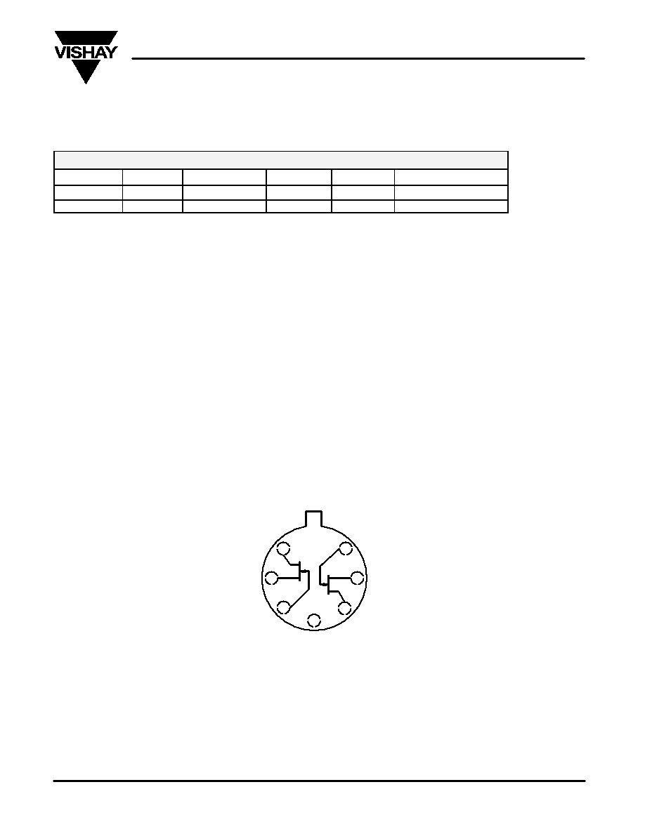
TO-78
Top View
G1
S1
D1
G2
D2
S2
Case
1
2
3
7
6
5
4
ABSOLUTE MAXIMUM RATINGS
Gate-Drain, Gate-Source Voltage
–25 V
. . . . . . . . . . . . . . . . . . . . . . . . . . . . . . .
Gate-Gate Voltage
"80 V
. . . . . . . . . . . . . . . . . . . . . . . . . . . . . . . . . . . . . . . . . . . .
Gate Current
50 mA
. . . . . . . . . . . . . . . . . . . . . . . . . . . . . . . . . . . . . . . . . . . . . . . . .
Lead Temperature (1/16” from case for 10 sec.)
300
_C
. . . . . . . . . . . . . . . . . . .
Storage Temperature
–65 to 200
_C
. . . . . . . . . . . . . . . . . . . . . . . . . . . . . . . . . . .
Operating Junction Temperature
–55 to 150
_C
. . . . . . . . . . . . . . . . . . . . . . . . . .
Power Dissipation :
Per Sidea
367 mW
. . . . . . . . . . . . . . . . . . . . . . . .
Totalb
500 mW
. . . . . . . . . . . . . . . . . . . . . . . . . . .
Notes
a.
Derate 3 mW/
_C above 25_C
b.
Derate 4 mW/
_C above 25_C
For applications information see AN102.
相关PDF资料 |
PDF描述 |
|---|---|
| 2N5944 | UHF BAND, Si, NPN, RF SMALL SIGNAL TRANSISTOR |
| 2N5945 | UHF BAND, Si, NPN, RF POWER TRANSISTOR |
| 2N5954 | 6 A, 80 V, PNP, Si, POWER TRANSISTOR, TO-66 |
| 2N5955 | 6 A, 60 V, PNP, Si, POWER TRANSISTOR, TO-66 |
| 2N5954 | 6 A, 85 V, PNP, Si, POWER TRANSISTOR, TO-66 |
相关代理商/技术参数 |
参数描述 |
|---|---|
| 2N5912 | 制造商:Vishay Siliconix 功能描述:TRANSISTOR JFET DUAL N TO-78 |
| 2N5912_TO-71 | 制造商:MICROSS 制造商全称:MICROSS 功能描述:MONOLITHIC DUAL N-CHANNEL JFET |
| 2N5912C_TO-71 | 制造商:MICROSS 制造商全称:MICROSS 功能描述:MONOLITHIC DUAL N-CHANNEL JFET |
| 2N5912-E3 | 功能描述:JFET 25V 1pA RoHS:否 制造商:ON Semiconductor 晶体管极性:N-Channel 漏极电流(Vgs=0 时的 Idss):50 mA 漏源电压 VDS:15 V 闸/源击穿电压: 漏极连续电流:50 mA 配置: 安装风格: 封装 / 箱体:SC-59 封装:Reel |
| 2N5913 | 制造商:STMicroelectronics 功能描述:2N5913 |
发布紧急采购,3分钟左右您将得到回复。