- 您现在的位置:买卖IC网 > PDF目录67338 > 5962-9561501MLX (ANALOG DEVICES INC) 8-CH 12-BIT PROPRIETARY METHOD ADC, SERIAL ACCESS, CDIP24 PDF资料下载
参数资料
| 型号: | 5962-9561501MLX |
| 厂商: | ANALOG DEVICES INC |
| 元件分类: | ADC |
| 英文描述: | 8-CH 12-BIT PROPRIETARY METHOD ADC, SERIAL ACCESS, CDIP24 |
| 封装: | 0.300 INCH, HERMETIC SEALED, CERDIP-24 |
| 文件页数: | 21/22页 |
| 文件大小: | 203K |
| 代理商: | 5962-9561501MLX |
REV. B
AD7890
–8–
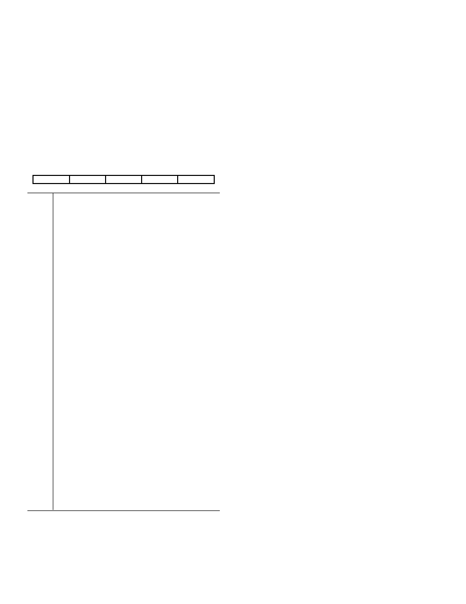
CONTROL REGISTER
The Control Register for the AD7890 contains 5 bits of informa-
tion as described below. Six serial clock pulses must be provided
to the part in order to write data to the Control Register (seven
if the write is required to put the part in Standby Mode). If
TFS
returns high before six serial clock cycles then no data transfer
takes place to the Control Register and the write cycle will have
to be restarted to write the data to the Control Register. If,
however, the CONV bit of the register (see below) is set to a
Logic 1, then a conversion will be initiated whenever a Control
Register write takes place regardless of how many serial clock
cycles the
TFS remains low for. The default (power-on) condi-
tion of all bits in the Control Register is 0.
MSB
A2
A1
A0
CONV
STBY
A2
Address Input. This input is the most significant
address input for multiplexer channel selection.
A1
Address Input. This is the 2nd most significant address
input for multiplexer channel selection.
A0
Address Input. Least significant address input for
multiplexer channel selection. When the address is
written to the control register, an internal pulse is
initiated, the pulsewidth of which is determined by
the value of capacitance on the CEXT pin. When this
pulse is active, it ensures the conversion process can-
not be activated. This allows for the multiplexer
settling time and track/hold acquisition time before
the track/hold goes into hold and conversion is initi-
ated. In applications where there is an anti-aliasing
filter between MUX OUT and SHA IN, the filter
settling time can be taken into account before the
input at SHA IN is sampled. When the internal pulse
times out, the track/hold goes into hold and conver-
sion is initiated.
CONV
Conversion Start. Writing a 1 to this bit initiates a
conversion in a similar manner to the
CONVST input.
Continuous conversion starts do not take place when
there is a 1 in this location. The internal pulse and
the conversion process are initiated after the sixth
serial clock cycle of the write operation if a 1 is written
to this bit. With a 1 in this bit, the hardware conver-
sion start i.e., the
CONVST input, is disabled. Writing
a 0 to this bit enables the hardware
CONVST input.
STBY
Standby Mode Input. Writing a 1 to this bit places
the device in its standby or power-down mode. Writ-
ing a 0 to this bit places the device in its normal
operating mode. The part does not enter its standby
mode until the seventh falling edge of SCLK in a
write operation. Therefore, the part requires seven
serial clock pulses in its serial write operation if it is
required to put the part into standby.
CONVERTER DETAILS
The AD7890 is an eight-channel, 12-bit, single supply, serial
data acquisition system. It provides the user with signal scaling,
multiplexer, track/hold, reference, A/D converter and versatile
serial logic functions on a single chip. The signal scaling allows
the part to handle
±10 V input signals (AD7890-10) and 0 V to
4.096 V input signals (AD7890-4) while operating from a single
5 V supply. The AD7890-2 contains no signal scaling and accepts
an analog input range of 0 V to 2.5 V. The part operates from
a 2.5 V reference which can be provided from the part’s own
internal reference or from an external reference source.
Unlike other single chip data acquisition solutions, the AD7890
provides the user with separate access to the multiplexer and the
A/D converter. This means that the flexibility of separate multi-
plexer and ADC solutions is not sacrificed with the one-chip
solution. With access to the multiplexer output, the user can
implement external signal conditioning between the multiplexer
and the track/hold. It means that one antialiasing filter can be
used on the output of the multiplexer to provide the antialiasing
function for all eight channels.
Conversion is initiated on the AD7890 either by pulsing the
CONVST input or by writing a Logic 1 to the CONV bit of the
Control Register. When using the hardware
CONVST input, on
the rising edge of the
CONVST signal, the on-chip track/hold
goes from track to hold mode and the conversion sequence is
started provided the internal pulse has timed out. This internal
pulse (which appears at the CEXT pin) is initiated whenever the
multiplexer address is loaded to the AD7890 Control Register.
This pulse goes from high to low when a serial write to the part
is initiated. It starts to discharge on the sixth falling clock edge
of SCLK in a serial write operation to the part. The track/hold
cannot go into hold and conversion cannot be initiated until the
CEXT pin has crossed its trigger point of 2.5 V. The discharge
time of the voltage on CEXT depends upon the value of capacitor
connected to the CEXT pin (see CEXT Functioning section). The
fact that the pulse is initiated every time a write to the control
register takes place means that the software conversion start and
track/hold signal is always delayed by the internal pulse.
The conversion clock for the part is generated from the clock
signal applied to the CLK IN pin of the part. Conversion time
for the AD7890 is 5.9
s from the rising edge of the hardware
CONVST signal and the track/hold acquisition time is 2
s. To
obtain optimum performance from the part, the data read
operation or Control Register write operation should not occur
during the conversion or during 500 ns prior to the next conver-
sion. This allows the part to operate at throughput rates up to
117 kHz in the external clocking mode and achieve data sheet
specifications. The part can operate at slightly higher throughput
rates (up to 127 kHz), again in external clocking mode with
degraded performance (see Timing and Control section). The
throughput rate for self-clocking mode is limited by the serial
clock rate to 78 kHz.
All unused inputs should be connected to a voltage within the
nominal analog input range to avoid noise pickup. On the
AD7890-10, if any one of the input channels which are not
being converted goes more negative than –12 V, it can interfere
with the conversion on the selected channel.
相关PDF资料 |
PDF描述 |
|---|---|
| 5962-9562301QXA | 16-CHANNEL, SGL ENDED MULTIPLEXER, CDIP28 |
| 5962-9562302QXA | 8-CHANNEL, DIFFERENTIAL MULTIPLEXER, CDIP28 |
| 5962-9562302QXA | 8-CHANNEL, DIFFERENTIAL MULTIPLEXER, CDIP28 |
| 5962-9566702MEX | DUAL, SERIAL INPUT LOADING, 12-BIT DAC, CDIP16 |
| 5962-9566701MEX | DUAL, SERIAL INPUT LOADING, 12-BIT DAC, CDIP16 |
相关代理商/技术参数 |
参数描述 |
|---|---|
| 5962-9562302Q2A | 制造商:Vishay Siliconix 功能描述:DUAL MARKED - DG407AZ/883 - Rail/Tube |
| 5962-9562901QCA | 制造商:Vishay Siliconix 功能描述:ANLG SW DUAL SPST 22V/36V 14CDIP - Rail/Tube |
| 5962-9563301Q2A | 制造商:Texas Instruments 功能描述:Pref DRVR Dual 4.5V to 5.5V 1375mW 20-Pin LCCC Tube 制造商:Rochester Electronics LLC 功能描述:- Bulk |
| 5962-9563301QPA | 制造商:Texas Instruments 功能描述:Pref DRVR Dual 4.5V to 5.5V 1050mW 8-Pin CDIP Tube 制造商:Rochester Electronics LLC 功能描述:- Bulk |
| 59629563901MGA | 制造商:AD 功能描述:AMP038JMD |
发布紧急采购,3分钟左右您将得到回复。