- 您现在的位置:买卖IC网 > PDF目录97839 > 71M6513-IGTR/F (MAXIM INTEGRATED PRODUCTS INC) SPECIALTY ANALOG CIRCUIT, PQFP100 PDF资料下载
参数资料
| 型号: | 71M6513-IGTR/F |
| 厂商: | MAXIM INTEGRATED PRODUCTS INC |
| 元件分类: | 模拟信号调理 |
| 英文描述: | SPECIALTY ANALOG CIRCUIT, PQFP100 |
| 封装: | LEAD FREE, LQFP-100 |
| 文件页数: | 67/104页 |
| 文件大小: | 1390K |
| 代理商: | 71M6513-IGTR/F |
第1页第2页第3页第4页第5页第6页第7页第8页第9页第10页第11页第12页第13页第14页第15页第16页第17页第18页第19页第20页第21页第22页第23页第24页第25页第26页第27页第28页第29页第30页第31页第32页第33页第34页第35页第36页第37页第38页第39页第40页第41页第42页第43页第44页第45页第46页第47页第48页第49页第50页第51页第52页第53页第54页第55页第56页第57页第58页第59页第60页第61页第62页第63页第64页第65页第66页当前第67页第68页第69页第70页第71页第72页第73页第74页第75页第76页第77页第78页第79页第80页第81页第82页第83页第84页第85页第86页第87页第88页第89页第90页第91页第92页第93页第94页第95页第96页第97页第98页第99页第100页第101页第102页第103页第104页
71M6513/71M6513H
3-Phase Energy Meter IC
DATA SHEET
SEPTEMBER 2011
2005-2011 Teridian Semiconductor Corporation
Page: 65 of 104
A Maxim Integrated Products Brand
Name
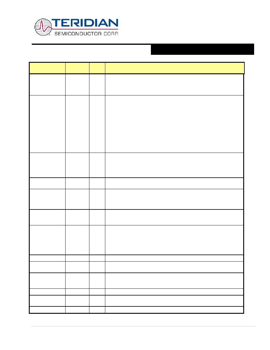
Location
[Bit(s)]
Dir
Description
PRE_SAMPS[1:0]
2001[7:6]
R/W
Together w/ SUM_CYCLES, this value determines the number of samples in
one sum cycle between XFER interrupts for the CE.
Number of samples = PRE_SAMPS*SUM_CYCLES.
00-42, 01-50, 10-84, 11-100
RTC_SEC[5:0]
RTC_MINI[5:0]
RTC_HR[4:0]
RTC_DAY[2:0]
RTC_DATE[4:0]
RTC_MO[3:0]
RTC_YR[7:0]
2015
2016
2017
2018
2019
201A
201B
R/W
The RTC interface. These are the ‘year’, ‘month’, ‘day’, ‘hour’, ‘minute’ and
‘second’ parameters for the RTC. The RTC is set by writing to these
registers. Year 00 is defined as a leap year.
SEC
00 to 59
MIN
00 to 59
HR
00 to 23 (00=Midnight)
DAY
01 to 07 (01=Sunday)
DATE 01 to 31
MO
01 to 12
YR
00 to 256
RTC_DEC_SEC
RTC_INC_SEC
201C[1]
201C[0]
W
RTC time correction bits. Only one bit may be pulsed at a time. When
pulsed, causes the RTC time value to be incremented (or decremented) by
an additional second the next time the RTC_SEC register is clocked. The
pulse width may be any value. If an additional correction is desired, the
MPU must wait 2 seconds before pulsing one of the bits again.
RTM_EN
2002[3]
R/W
Real Time Monitor enable. When ‘0’, the RTM output is low. This bit
enables the two wire version of RTM
RTM0[7:0]
RTM1[7:0]
RTM2[7:0]
RTM3[7:0]
2060
2061
2062
2063
R/W
Four RTM probes. Before each CE code pass, the values of these registers
are serially output on the RTM pin. The RTM registers are ignored when
RTM_EN=0.
SECURE
SFR B2[6]
R/W
Enables security provisions that prevent external reading of flash memory
and CE program RAM. This bit is reset on chip reset and may only be set.
Attempts to write zero are ignored.
SSI_EN
2070[7]
R/W
Enables the Synchronous Serial Interface (SSI) on SEG3, SEG4, and
SEG5 pins. If SSI_RDYEN is set, SEG6 is enabled also. The pins take on the
new functions SCLK, SSDATA, SFR, and SRDY, respectively. When
SSI_EN is high and LCD_EN is low, these pins are converted to the SSI
function, regardless of LCDEN and LCD_NUM. For proper LCD operation,
SSI_EN must not be high when LCD_EN is high.
SSI_10M
2070[6]
R/W
SSI clock speed: 0: 5MHz, 1: 10MHz
SSI_CKGATE
2070[5]
R/W
SSI gated clock enable. When low, the SCLK is continuous. When high, the
clock is held low when data is not being transferred.
SSI_FSIZE[1:0]
2070[4:3]
R/W
SSI frame pulse format:
0: once at beginning of SSI sequence (whole block of data),
1: every 8 bits, 2: every 16 bits, 3: every 32 bits.
SSI_FPOL
2070[2]
R/W
SFR pulse polarity: 0: positive, 1: negative
SSI_RDYEN
2070[1]
R/W
SRDY enable. If SSI_RDYEN and SSI_EN are high, the SEG6 pin is
configured as SRDY. Otherwise, it is an LCD driver.
SSI_RDYPOL
2070[0]
R/W
SRDY polarity: 0: positive, 1: negative
相关PDF资料 |
PDF描述 |
|---|---|
| 71M6513H-IGT/F | SPECIALTY ANALOG CIRCUIT, PQFP100 |
| 71M6513H-IGTR/F | SPECIALTY ANALOG CIRCUIT, PQFP100 |
| 71M6513-IGT/F | SPECIALTY ANALOG CIRCUIT, PQFP100 |
| 71M6515H-IGTW/F | SPECIALTY ANALOG CIRCUIT, PQFP64 |
| 71M6515H-IGTWR/F | SPECIALTY ANALOG CIRCUIT, PQFP64 |
相关代理商/技术参数 |
参数描述 |
|---|---|
| 71M6515H | 制造商:TERIDIAN 制造商全称:TERIDIAN 功能描述:Energy Meter IC |
| 71M6515H_11 | 制造商:TERIDIAN 制造商全称:TERIDIAN 功能描述:Up to 10ppmC precision ultra-stable voltage reference Digital temperature compensation |
| 71M6515H-DB | 功能描述:开发板和工具包 - 8051 71M6515H Demo Brd RoHS:否 制造商:Silicon Labs 产品:Development Kits 工具用于评估:C8051F960, Si7005 核心: 接口类型:USB 工作电源电压: |
| 71M6515H-IGT | 制造商:Maxim Integrated Products 功能描述:METERING FRONT END - Rail/Tube |
| 71M6515H-IGT/F | 功能描述:计量片上系统 - SoC Energy Meter IC RoHS:否 制造商:Maxim Integrated 核心:80515 MPU 处理器系列:71M6511 类型:Metering SoC 最大时钟频率:70 Hz 程序存储器大小:64 KB 数据 RAM 大小:7 KB 接口类型:UART 可编程输入/输出端数量:12 片上 ADC: 安装风格:SMD/SMT 封装 / 箱体:LQFP-64 封装:Reel |
发布紧急采购,3分钟左右您将得到回复。