- 您现在的位置:买卖IC网 > PDF目录294128 > 72V285L15TFI9 (INTEGRATED DEVICE TECHNOLOGY INC) 64K X 18 OTHER FIFO, 10 ns, PQFP64 PDF资料下载
参数资料
| 型号: | 72V285L15TFI9 |
| 厂商: | INTEGRATED DEVICE TECHNOLOGY INC |
| 元件分类: | FIFO |
| 英文描述: | 64K X 18 OTHER FIFO, 10 ns, PQFP64 |
| 封装: | STQFP-64 |
| 文件页数: | 16/25页 |
| 文件大小: | 266K |
| 代理商: | 72V285L15TFI9 |
23
COMMERCIAL AND INDUSTRIAL
TEMPERATURERANGES
IDT72V275/72V285 3.3V CMOS SUPERSYNC FIFOTM
32,768 x 18 and 65,536 x 18
NOTES:
1. Use an AND gate in IDT Standard mode, an OR gate in FWFT mode.
2. Do not connect any output control signals directly together.
3. FIFO #1 and FIFO #2 must be the same depth, but may be different word widths.
OPTIONAL CONFIGURATIONS
WIDTH EXPANSION CONFIGURATION
Word width may be increased simply by connecting together the control
signals of multiple devices. Status flags can be detected from any one
device. The exceptions are the
EF and FF functions in IDT Standard mode
and the
IRand OR functions in FWFT mode. Because of variations in skew
between RCLK and WCLK, it is possible for
EF/FF deassertion and IR/
OR assertion to vary by one cycle between FIFOs. In IDT Standard mode,
such problems can be avoided by creating composite flags, that is, ANDing
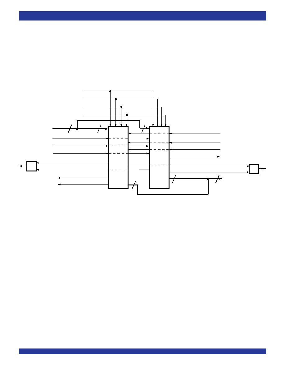
Figure 19. Block Diagram of 32,768 x 36 and 65,536 x 36 Width Expansion
DEPTH EXPANSION CONFIGURATION (FWFT MODE ONLY)
The IDT72V275 can easily be adapted to applications requiring depths
greater than 32,768 and 65,536 for the IDT72V285 with an 18-bit bus width.
In FWFT mode, the FIFOs can be connected in series (the data outputs of one
FIFOconnectedtothedatainputsofthenext)withnoexternallogicnecessary.
The resulting configuration provides a total depth equivalent to the sum of the
depths associated with each single FIFO. Figure 20 shows a depth expansion
using two IDT72V275/72V285 devices.
CareshouldbetakentoselectFWFTmodeduringMasterResetforallFIFOs
in the depth expansion configuration. The first word written to an empty
configuration will pass from one FIFO to the next ("ripple down") until it finally
appears at the outputs of the last FIFO in the chain–no read operation is
necessarybuttheRCLKofeachFIFOmustbefree-running. Eachtimethedata
word appears at the outputs of one FIFO, that device's
OR line goes LOW,
enabling a write to the next FIFO in line.
For an empty expansion configuration, the amount of time it takes for
ORof
the last FIFO in the chain to go LOW (i.e. valid data to appear on the last FIFO's
outputs) after a word has been written to the first FIFO is the sum of the delays
for each individual FIFO:
(N – 1)*(4*transfer clock) + 3*TRCLK
whereNisthenumberofFIFOsintheexpansionandTRCLK istheRCLKperiod.
Note that extra cycles should be added for the possibility that the tSKEW3
specificationisnotmetbetweenWCLKandtransferclock,orRCLKandtransfer
clock, for the
ORflag.
The"rippledown"delayisonlynoticeableforthefirstwordwrittentoanempty
depth expansion configuration. There will be no delay evident for subsequent
words written to the configuration.
The first free location created by reading from a full depth expansion
configurationwill"bubbleup"fromthelastFIFOtothepreviousoneuntilitfinally
movesintothefirstFIFOofthechain. Eachtimeafreelocationiscreatedinone
FIFO of the chain, that FIFO's
IRlinegoesLOW,enablingtheprecedingFIFO
to write a word to fill it.
EFofeveryFIFO,andseparatelyANDingFFofeveryFIFO. InFWFTmode,
composite flags can be created by ORing
OR of every FIFO, and separately
ORing
IR of every FIFO.
Figure 19 demonstrates a width expansion using two IDT72V275/72V285
devices. D0 - D17 from each device form a 36-bit wide input bus and Q0-Q17
fromeachdeviceforma36-bitwideoutputbus.Anywordwidthcanbeattained
by adding additional IDT72V275/72V285 devices.
WRITE CLOCK (WCLK)
m + n
m
n
MASTER RESET (
MRS)
READ CLOCK (RCLK)
DATA OUT
n
m + n
WRITE ENABLE (
WEN)
FULL FLAG/INPUT READY (
FF/IR)
PROGRAMMABLE (
PAF)
PROGRAMMABLE (
PAE)
EMPTY FLAG/OUTPUT READY (
EF/OR) #2
OUTPUT ENABLE (
OE)
READ ENABLE (
REN)
m
LOAD (
LD)
IDT
72V275
72V285
EMPTY FLAG/OUTPUT READY (
EF/OR) #1
PARTIAL RESET (
PRS)
IDT
72V275
72V285
4512 drw 22
FULL FLAG/INPUT READY (
FF/IR) #2
HALF-FULL FLAG (
HF)
FIRST WORD FALL THROUGH/
SERIAL INPUT (FWFT/SI)
RETRANSMIT (
RT)
#1
FIFO
#2
GATE
(1)
GATE
(1)
D0 - Dm
DATA IN
Dm+1 - Dn
Q0 - Qm
Qm+1 - Qn
FIFO
#1
相关PDF资料 |
PDF描述 |
|---|---|
| 72V3626L15PFG | 256 X 36 BI-DIRECTIONAL FIFO, 10 ns, PQFP128 |
| 72V3684L15PF | 16K X 36 BI-DIRECTIONAL FIFO, 10 ns, PQFP128 |
| 72V845L15PFI8 | 4K X 18 BI-DIRECTIONAL FIFO, 10 ns, PQFP128 |
| 72V805L15PFI9 | 256 X 18 BI-DIRECTIONAL FIFO, 10 ns, PQFP128 |
| 72V805L15PF8 | 256 X 18 BI-DIRECTIONAL FIFO, 10 ns, PQFP128 |
相关代理商/技术参数 |
参数描述 |
|---|---|
| 72V285L20PF | 功能描述:先进先出 RoHS:否 制造商:IDT 电路数量: 数据总线宽度:18 bit 总线定向:Unidirectional 存储容量:4 Mbit 定时类型:Synchronous 组织:256 K x 18 最大时钟频率:100 MHz 访问时间:10 ns 电源电压-最大:3.6 V 电源电压-最小:6 V 最大工作电流:35 mA 最大工作温度:+ 85 C 封装 / 箱体:TQFP-80 封装: |
| 72V285L20PF8 | 制造商:Integrated Device Technology Inc 功能描述:FIFO Mem Sync Dual Depth/Width Uni-Dir 64K x 18 64-Pin TQFP T/R 制造商:Integrated Device Technology Inc 功能描述:FIFO SYNC DUAL DEPTH/WIDTH UNI-DIR 64KX18 64TQFP - Tape and Reel |
| 72V285L20TF | 功能描述:先进先出 RoHS:否 制造商:IDT 电路数量: 数据总线宽度:18 bit 总线定向:Unidirectional 存储容量:4 Mbit 定时类型:Synchronous 组织:256 K x 18 最大时钟频率:100 MHz 访问时间:10 ns 电源电压-最大:3.6 V 电源电压-最小:6 V 最大工作电流:35 mA 最大工作温度:+ 85 C 封装 / 箱体:TQFP-80 封装: |
| 72V285L20TF8 | 制造商:Integrated Device Technology Inc 功能描述:FIFO SYNC DUAL DEPTH/WIDTH UNI-DIR 64KX18 64TQFP - Tape and Reel |
| 72V291L10PF | 功能描述:先进先出 RoHS:否 制造商:IDT 电路数量: 数据总线宽度:18 bit 总线定向:Unidirectional 存储容量:4 Mbit 定时类型:Synchronous 组织:256 K x 18 最大时钟频率:100 MHz 访问时间:10 ns 电源电压-最大:3.6 V 电源电压-最小:6 V 最大工作电流:35 mA 最大工作温度:+ 85 C 封装 / 箱体:TQFP-80 封装: |
发布紧急采购,3分钟左右您将得到回复。