- 您现在的位置:买卖IC网 > PDF目录253905 > A3P015-1QNG68I FPGA, 384 CLBS, 15000 GATES, QCC68 PDF资料下载
参数资料
| 型号: | A3P015-1QNG68I |
| 元件分类: | FPGA |
| 英文描述: | FPGA, 384 CLBS, 15000 GATES, QCC68 |
| 封装: | 8 X 8 MM, 0.90 MM HEIGHT, 0.40 MM PITCH, GREEN, QFN-68 |
| 文件页数: | 13/218页 |
| 文件大小: | 6270K |
| 代理商: | A3P015-1QNG68I |
第1页第2页第3页第4页第5页第6页第7页第8页第9页第10页第11页第12页当前第13页第14页第15页第16页第17页第18页第19页第20页第21页第22页第23页第24页第25页第26页第27页第28页第29页第30页第31页第32页第33页第34页第35页第36页第37页第38页第39页第40页第41页第42页第43页第44页第45页第46页第47页第48页第49页第50页第51页第52页第53页第54页第55页第56页第57页第58页第59页第60页第61页第62页第63页第64页第65页第66页第67页第68页第69页第70页第71页第72页第73页第74页第75页第76页第77页第78页第79页第80页第81页第82页第83页第84页第85页第86页第87页第88页第89页第90页第91页第92页第93页第94页第95页第96页第97页第98页第99页第100页第101页第102页第103页第104页第105页第106页第107页第108页第109页第110页第111页第112页第113页第114页第115页第116页第117页第118页第119页第120页第121页第122页第123页第124页第125页第126页第127页第128页第129页第130页第131页第132页第133页第134页第135页第136页第137页第138页第139页第140页第141页第142页第143页第144页第145页第146页第147页第148页第149页第150页第151页第152页第153页第154页第155页第156页第157页第158页第159页第160页第161页第162页第163页第164页第165页第166页第167页第168页第169页第170页第171页第172页第173页第174页第175页第176页第177页第178页第179页第180页第181页第182页第183页第184页第185页第186页第187页第188页第189页第190页第191页第192页第193页第194页第195页第196页第197页第198页第199页第200页第201页第202页第203页第204页第205页第206页第207页第208页第209页第210页第211页第212页第213页第214页第215页第216页第217页第218页
ProASIC3 Device Family Overview
v1.3
1 - 7
I/Os with Advanced I/O Standards
The ProASIC3 family of FPGAs features a flexible I/O structure, supporting a range of voltages
(1.5 V, 1.8 V, 2.5 V, and 3.3 V). ProASIC3 FPGAs support many different I/O standards—single-ended
and differential.
The I/Os are organized into banks, with two or four banks per device. The configuration of these
banks determines the I/O standards supported (Table 1-1).
Each I/O module contains several input, output, and enable registers. These registers allow the
implementation of the following:
Single-Data-Rate applications
Double-Data-Rate applications—DDR LVDS, B-LVDS, and M-LVDS I/Os for point-to-point
communications
ProASIC3 banks for the A3P250 device and above support LVPECL, LVDS, B-LVDS and M-LVDS.
B-LVDS and M-LVDS can support up to 20 loads.
Hot-swap (also called hot-plug, or hot-insertion) is the operation of hot-insertion or hot-removal of
a card in a powered-up system.
Cold-sparing (also called cold-swap) refers to the ability of a device to leave system data
undisturbed when the system is powered up, while the component itself is powered down, or
when power supplies are floating.
Wide Range I/O Support
Actel ProASIC3 devices support JEDEC-defined wide range I/O operation. ProASIC3 supports the
JESD8-B specification, covering both 3 V and 3.3 V supplies, for an effective operating range of
2.7 V to 3.6 V.
Wider I/O range means designers can eliminate power supplies or power conditioning components
from the board or move to less costly components with greater tolerances. Wide range eases I/O
bank management and provides enhanced protection from system voltage spikes, while providing
the flexibility to easily run custom voltage applications.
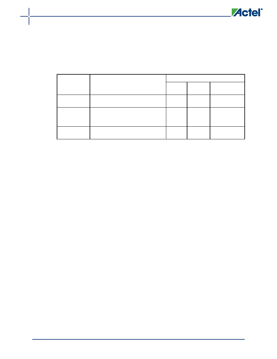
Table 1-1
I/O Standards Supported
I/O Bank Type
Device and Bank Location
I/O Standards Supported
LVTTL/
LVCMOS
PCI/PCI-X
LVPECL, LVDS,
B-LVDS, M-LVDS
Advanced
East and west Banks of A3P250 and
larger devices
Standard Plus
North and south banks of A3P250 and
larger devices
All banks of A3P060 and A3P125
Not supported
Standard
All banks of A3P015 and A3P030
Not
supported
Not supported
相关PDF资料 |
PDF描述 |
|---|---|
| A3P015-1QNG68 | FPGA, 384 CLBS, 15000 GATES, 350 MHz, QCC68 |
| A3P015-2QN68I | FPGA, 384 CLBS, 15000 GATES, QCC68 |
| A3P015-2QN68 | FPGA, 384 CLBS, 15000 GATES, 350 MHz, QCC68 |
| A3P015-2QNG68I | FPGA, 384 CLBS, 15000 GATES, QCC68 |
| A3P015-2QNG68 | FPGA, 384 CLBS, 15000 GATES, 350 MHz, QCC68 |
相关代理商/技术参数 |
参数描述 |
|---|---|
| A3P015-1VQ144 | 制造商:ACTEL 制造商全称:Actel Corporation 功能描述:ProASIC3 Flash Family FPGAs |
| A3P015-1VQ144ES | 制造商:ACTEL 制造商全称:Actel Corporation 功能描述:ProASIC3 Flash Family FPGAs |
| A3P015-1VQ144I | 制造商:ACTEL 制造商全称:Actel Corporation 功能描述:ProASIC3 Flash Family FPGAs |
| A3P015-1VQ144PP | 制造商:ACTEL 制造商全称:Actel Corporation 功能描述:ProASIC3 Flash Family FPGAs |
| A3P015-1VQG144 | 制造商:ACTEL 制造商全称:Actel Corporation 功能描述:ProASIC3 Flash Family FPGAs |
发布紧急采购,3分钟左右您将得到回复。