- 您现在的位置:买卖IC网 > PDF目录253905 > A3P015-1QNG68I FPGA, 384 CLBS, 15000 GATES, QCC68 PDF资料下载
参数资料
| 型号: | A3P015-1QNG68I |
| 元件分类: | FPGA |
| 英文描述: | FPGA, 384 CLBS, 15000 GATES, QCC68 |
| 封装: | 8 X 8 MM, 0.90 MM HEIGHT, 0.40 MM PITCH, GREEN, QFN-68 |
| 文件页数: | 202/218页 |
| 文件大小: | 6270K |
| 代理商: | A3P015-1QNG68I |
第1页第2页第3页第4页第5页第6页第7页第8页第9页第10页第11页第12页第13页第14页第15页第16页第17页第18页第19页第20页第21页第22页第23页第24页第25页第26页第27页第28页第29页第30页第31页第32页第33页第34页第35页第36页第37页第38页第39页第40页第41页第42页第43页第44页第45页第46页第47页第48页第49页第50页第51页第52页第53页第54页第55页第56页第57页第58页第59页第60页第61页第62页第63页第64页第65页第66页第67页第68页第69页第70页第71页第72页第73页第74页第75页第76页第77页第78页第79页第80页第81页第82页第83页第84页第85页第86页第87页第88页第89页第90页第91页第92页第93页第94页第95页第96页第97页第98页第99页第100页第101页第102页第103页第104页第105页第106页第107页第108页第109页第110页第111页第112页第113页第114页第115页第116页第117页第118页第119页第120页第121页第122页第123页第124页第125页第126页第127页第128页第129页第130页第131页第132页第133页第134页第135页第136页第137页第138页第139页第140页第141页第142页第143页第144页第145页第146页第147页第148页第149页第150页第151页第152页第153页第154页第155页第156页第157页第158页第159页第160页第161页第162页第163页第164页第165页第166页第167页第168页第169页第170页第171页第172页第173页第174页第175页第176页第177页第178页第179页第180页第181页第182页第183页第184页第185页第186页第187页第188页第189页第190页第191页第192页第193页第194页第195页第196页第197页第198页第199页第200页第201页当前第202页第203页第204页第205页第206页第207页第208页第209页第210页第211页第212页第213页第214页第215页第216页第217页第218页
ProASIC3 DC and Switching Characteristics
2- 70
v1.4
LVPECL
Low-Voltage Positive Emitter-Coupled Logic (LVPECL) is another differential I/O standard. It
requires that one data bit be carried through two signal lines. Like LVDS, two pins are needed. It
also requires external resistor termination.
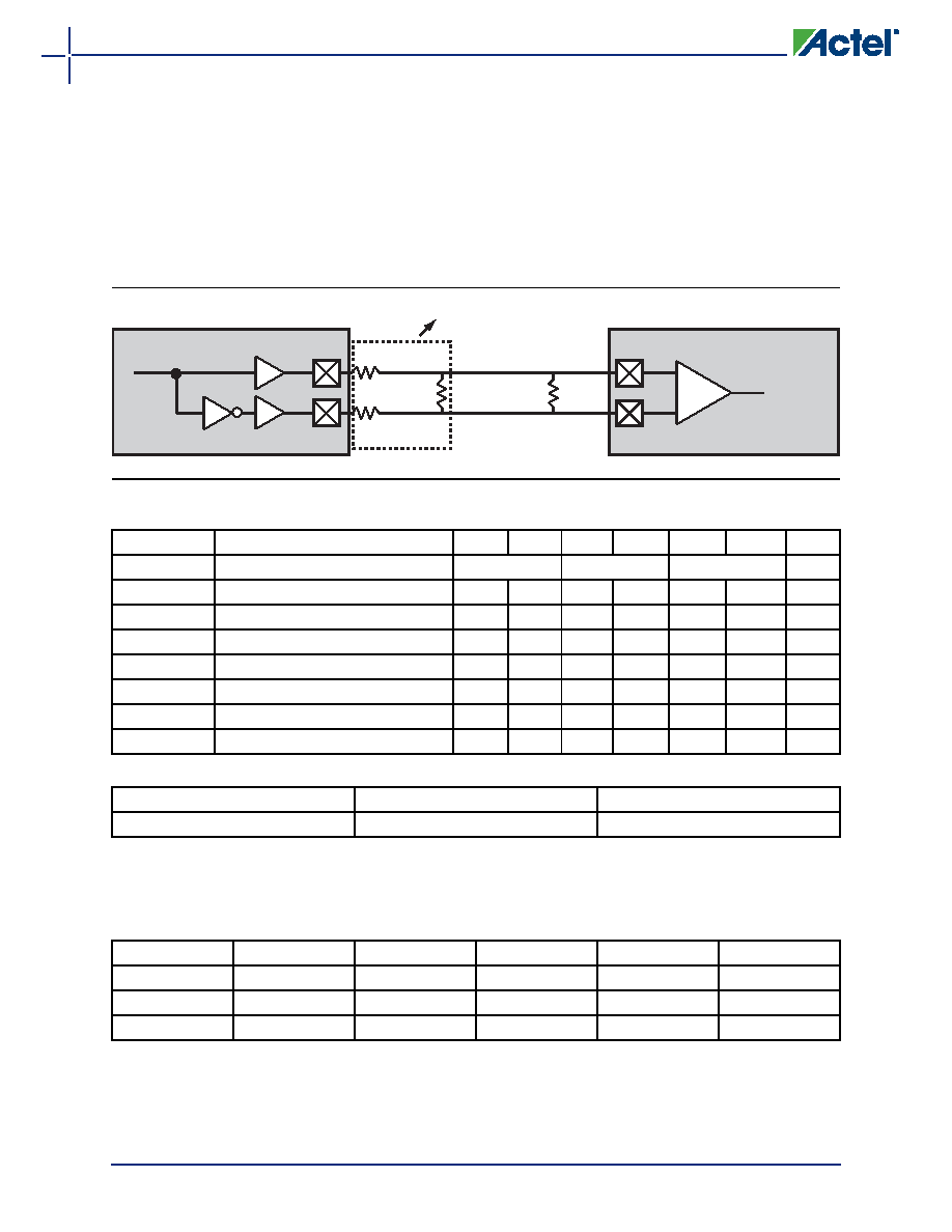
The full implementation of the LVDS transmitter and receiver is shown in an example in
Figure 2-13. The building blocks of the LVPECL transmitter-receiver are one transmitter macro, one
receiver macro, three board resistors at the transmitter end, and one resistor at the receiver end.
The values for the three driver resistors are different from those used in the LVDS implementation
because the output standard specifications are different.
Timing Characteristics
Figure 2-13 LVPECL Circuit Diagram and Board-Level Implementation
Table 2-93 Minimum and Maximum DC Input and Output Levels
DC Parameter
Description
Min.
Max.
Min.
Max.
Min.
Max.
Units
VCCI
Supply Voltage
3.0
3.3
3.6
V
VOL
Output LOW Voltage
0.96
1.27
1.06
1.43
1.30
1.57
V
VOH
Output HIGH Voltage
1.8
2.11
1.92
2.28
2.13
2.41
V
VIL, VIH
Input LOW, Input HIGH Voltages
0
3.3
0
3.6
0
3.9
V
VODIFF
Differential Output Voltage
0.625
0.97
0.625
0.97
0.625
0.97
V
VOCM
Output Common-Mode Voltage
1.762
1.98
1.762
1.98
1.762
1.98
V
VICM
Input Common-Mode Voltage
1.01
2.57
1.01
2.57
1.01
2.57
V
VIDIFF
Input Differential Voltage
300
mV
Table 2-94 AC Waveforms, Measuring Points, and Capacitive Loads
Input LOW (V)
Input HIGH (V)
Measuring Point* (V)
1.64
1.94
Cross point
187 W
100
Ω
Z0 = 50 Ω
100
Ω
100
Ω
+
–
P
N
P
N
INBUF_LVPECL
OUTBUF_LVPECL
FPGA
Bourns Part Number: CAT16-PC4F12
Table 2-95 LVPECL
Commercial-Case Conditions: TJ = 70°C, Worst-Case VCC = 1.425 V, Worst-Case VCCI = 3.0 V
Speed Grade
tDOUT
tDP
tDIN
tPY
Units
Std.
0.66
1.80
0.04
1.40
ns
–1
0.56
1.53
0.04
1.19
ns
–2
0.49
1.34
0.03
1.05
ns
Note: For specific junction temperature and voltage supply levels, refer to Table 2-6 on page 2-6 for derating
values.
相关PDF资料 |
PDF描述 |
|---|---|
| A3P015-1QNG68 | FPGA, 384 CLBS, 15000 GATES, 350 MHz, QCC68 |
| A3P015-2QN68I | FPGA, 384 CLBS, 15000 GATES, QCC68 |
| A3P015-2QN68 | FPGA, 384 CLBS, 15000 GATES, 350 MHz, QCC68 |
| A3P015-2QNG68I | FPGA, 384 CLBS, 15000 GATES, QCC68 |
| A3P015-2QNG68 | FPGA, 384 CLBS, 15000 GATES, 350 MHz, QCC68 |
相关代理商/技术参数 |
参数描述 |
|---|---|
| A3P015-1VQ144 | 制造商:ACTEL 制造商全称:Actel Corporation 功能描述:ProASIC3 Flash Family FPGAs |
| A3P015-1VQ144ES | 制造商:ACTEL 制造商全称:Actel Corporation 功能描述:ProASIC3 Flash Family FPGAs |
| A3P015-1VQ144I | 制造商:ACTEL 制造商全称:Actel Corporation 功能描述:ProASIC3 Flash Family FPGAs |
| A3P015-1VQ144PP | 制造商:ACTEL 制造商全称:Actel Corporation 功能描述:ProASIC3 Flash Family FPGAs |
| A3P015-1VQG144 | 制造商:ACTEL 制造商全称:Actel Corporation 功能描述:ProASIC3 Flash Family FPGAs |
发布紧急采购,3分钟左右您将得到回复。