- 您现在的位置:买卖IC网 > PDF目录253905 > A3P015-1QNG68I FPGA, 384 CLBS, 15000 GATES, QCC68 PDF资料下载
参数资料
| 型号: | A3P015-1QNG68I |
| 元件分类: | FPGA |
| 英文描述: | FPGA, 384 CLBS, 15000 GATES, QCC68 |
| 封装: | 8 X 8 MM, 0.90 MM HEIGHT, 0.40 MM PITCH, GREEN, QFN-68 |
| 文件页数: | 208/218页 |
| 文件大小: | 6270K |
| 代理商: | A3P015-1QNG68I |
第1页第2页第3页第4页第5页第6页第7页第8页第9页第10页第11页第12页第13页第14页第15页第16页第17页第18页第19页第20页第21页第22页第23页第24页第25页第26页第27页第28页第29页第30页第31页第32页第33页第34页第35页第36页第37页第38页第39页第40页第41页第42页第43页第44页第45页第46页第47页第48页第49页第50页第51页第52页第53页第54页第55页第56页第57页第58页第59页第60页第61页第62页第63页第64页第65页第66页第67页第68页第69页第70页第71页第72页第73页第74页第75页第76页第77页第78页第79页第80页第81页第82页第83页第84页第85页第86页第87页第88页第89页第90页第91页第92页第93页第94页第95页第96页第97页第98页第99页第100页第101页第102页第103页第104页第105页第106页第107页第108页第109页第110页第111页第112页第113页第114页第115页第116页第117页第118页第119页第120页第121页第122页第123页第124页第125页第126页第127页第128页第129页第130页第131页第132页第133页第134页第135页第136页第137页第138页第139页第140页第141页第142页第143页第144页第145页第146页第147页第148页第149页第150页第151页第152页第153页第154页第155页第156页第157页第158页第159页第160页第161页第162页第163页第164页第165页第166页第167页第168页第169页第170页第171页第172页第173页第174页第175页第176页第177页第178页第179页第180页第181页第182页第183页第184页第185页第186页第187页第188页第189页第190页第191页第192页第193页第194页第195页第196页第197页第198页第199页第200页第201页第202页第203页第204页第205页第206页第207页当前第208页第209页第210页第211页第212页第213页第214页第215页第216页第217页第218页
ProASIC3 Device Family Overview
v1.3
1 - 5
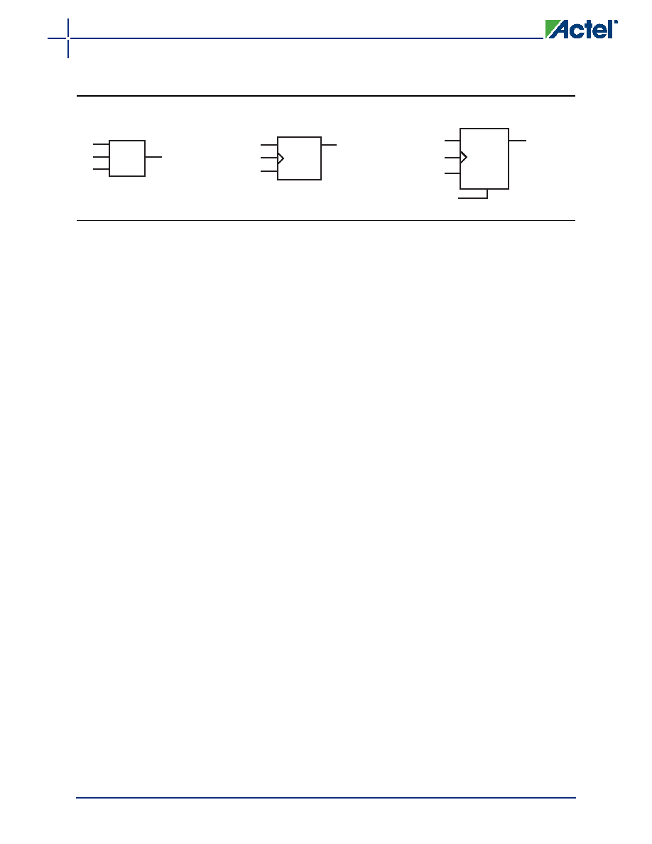
Refer to Figure 1-3 for VersaTile configurations.
User Nonvolatile FlashROM
Actel ProASIC3 devices have 1 kbit of on-chip, user-accessible, nonvolatile FlashROM. The FlashROM
can be used in diverse system applications:
Internet protocol addressing (wireless or fixed)
System calibration settings
Device serialization and/or inventory control
Subscription-based business models (for example, set-top boxes)
Secure key storage for secure communications algorithms
Asset management/tracking
Date stamping
Version management
The FlashROM is written using the standard ProASIC3 IEEE 1532 JTAG programming interface. The
core can be individually programmed (erased and written), and on-chip AES decryption can be used
selectively to securely load data over public networks (except in the A3P015 and A3P030 devices),
as in security keys stored in the FlashROM for a user design.
The FlashROM can be programmed via the JTAG programming interface, and its contents can be
read back either through the JTAG programming interface or via direct FPGA core addressing. Note
that the FlashROM can only be programmed from the JTAG interface and cannot be programmed
from the internal logic array.
The FlashROM is programmed as 8 banks of 128 bits; however, reading is performed on a byte-by-
byte basis using a synchronous interface. A 7-bit address from the FPGA core defines which of the 8
banks and which of the 16 bytes within that bank are being read. The three most significant bits
(MSBs) of the FlashROM address determine the bank, and the four least significant bits (LSBs) of
the FlashROM address define the byte.
The Actel ProASIC3 development software solutions, Libero Integrated Design Environment (IDE)
and Designer, have extensive support for the FlashROM. One such feature is auto-generation of
sequential programming files for applications requiring a unique serial number in each part.
Another feature allows the inclusion of static data for system version control. Data for the
FlashROM can be generated quickly and easily using Actel Libero IDE and Designer software tools.
Comprehensive programming file support is also included to allow for easy programming of large
numbers of parts with differing FlashROM contents.
SRAM and FIFO
ProASIC3 devices (except the A3P015 and A3P030 devices) have embedded SRAM blocks along their
north and south sides. Each variable-aspect-ratio SRAM block is 4,608 bits in size. Available memory
configurations are 256×18, 512×9, 1k×4, 2k×2, and 4k×1 bits. The individual blocks have
independent read and write ports that can be configured with different bit widths on each port.
For example, data can be sent through a 4-bit port and read as a single bitstream. The embedded
SRAM blocks can be initialized via the device JTAG port (ROM emulation mode) using the UJTAG
macro (except in A3P015 and A3P030 devices).
Figure 1-3 VersaTile Configurations
X1
Y
X2
X3
LUT-3
Data
Y
CLK
Enable
CLR
D-FF
Data
Y
CLK
CLR
D-FF
LUT-3 Equivalent
D-Flip-Flop with Clear or Set
Enable D-Flip-Flop with Clear or Set
相关PDF资料 |
PDF描述 |
|---|---|
| A3P015-1QNG68 | FPGA, 384 CLBS, 15000 GATES, 350 MHz, QCC68 |
| A3P015-2QN68I | FPGA, 384 CLBS, 15000 GATES, QCC68 |
| A3P015-2QN68 | FPGA, 384 CLBS, 15000 GATES, 350 MHz, QCC68 |
| A3P015-2QNG68I | FPGA, 384 CLBS, 15000 GATES, QCC68 |
| A3P015-2QNG68 | FPGA, 384 CLBS, 15000 GATES, 350 MHz, QCC68 |
相关代理商/技术参数 |
参数描述 |
|---|---|
| A3P015-1VQ144 | 制造商:ACTEL 制造商全称:Actel Corporation 功能描述:ProASIC3 Flash Family FPGAs |
| A3P015-1VQ144ES | 制造商:ACTEL 制造商全称:Actel Corporation 功能描述:ProASIC3 Flash Family FPGAs |
| A3P015-1VQ144I | 制造商:ACTEL 制造商全称:Actel Corporation 功能描述:ProASIC3 Flash Family FPGAs |
| A3P015-1VQ144PP | 制造商:ACTEL 制造商全称:Actel Corporation 功能描述:ProASIC3 Flash Family FPGAs |
| A3P015-1VQG144 | 制造商:ACTEL 制造商全称:Actel Corporation 功能描述:ProASIC3 Flash Family FPGAs |
发布紧急采购,3分钟左右您将得到回复。