- 您现在的位置:买卖IC网 > PDF目录253905 > A3P015-1QNG68I FPGA, 384 CLBS, 15000 GATES, QCC68 PDF资料下载
参数资料
| 型号: | A3P015-1QNG68I |
| 元件分类: | FPGA |
| 英文描述: | FPGA, 384 CLBS, 15000 GATES, QCC68 |
| 封装: | 8 X 8 MM, 0.90 MM HEIGHT, 0.40 MM PITCH, GREEN, QFN-68 |
| 文件页数: | 90/218页 |
| 文件大小: | 6270K |
| 代理商: | A3P015-1QNG68I |
第1页第2页第3页第4页第5页第6页第7页第8页第9页第10页第11页第12页第13页第14页第15页第16页第17页第18页第19页第20页第21页第22页第23页第24页第25页第26页第27页第28页第29页第30页第31页第32页第33页第34页第35页第36页第37页第38页第39页第40页第41页第42页第43页第44页第45页第46页第47页第48页第49页第50页第51页第52页第53页第54页第55页第56页第57页第58页第59页第60页第61页第62页第63页第64页第65页第66页第67页第68页第69页第70页第71页第72页第73页第74页第75页第76页第77页第78页第79页第80页第81页第82页第83页第84页第85页第86页第87页第88页第89页当前第90页第91页第92页第93页第94页第95页第96页第97页第98页第99页第100页第101页第102页第103页第104页第105页第106页第107页第108页第109页第110页第111页第112页第113页第114页第115页第116页第117页第118页第119页第120页第121页第122页第123页第124页第125页第126页第127页第128页第129页第130页第131页第132页第133页第134页第135页第136页第137页第138页第139页第140页第141页第142页第143页第144页第145页第146页第147页第148页第149页第150页第151页第152页第153页第154页第155页第156页第157页第158页第159页第160页第161页第162页第163页第164页第165页第166页第167页第168页第169页第170页第171页第172页第173页第174页第175页第176页第177页第178页第179页第180页第181页第182页第183页第184页第185页第186页第187页第188页第189页第190页第191页第192页第193页第194页第195页第196页第197页第198页第199页第200页第201页第202页第203页第204页第205页第206页第207页第208页第209页第210页第211页第212页第213页第214页第215页第216页第217页第218页
ProASIC3 DC and Switching Characteristics
2- 4
v1.4
Power-Up/-Down Behavior of Low-Power Flash Devices chapter of the handbook for information
on clock and lock recovery.
Internal Power-Up Activation Sequence
1. Core
2. Input buffers
Output buffers, after 200 ns delay from input buffer activation
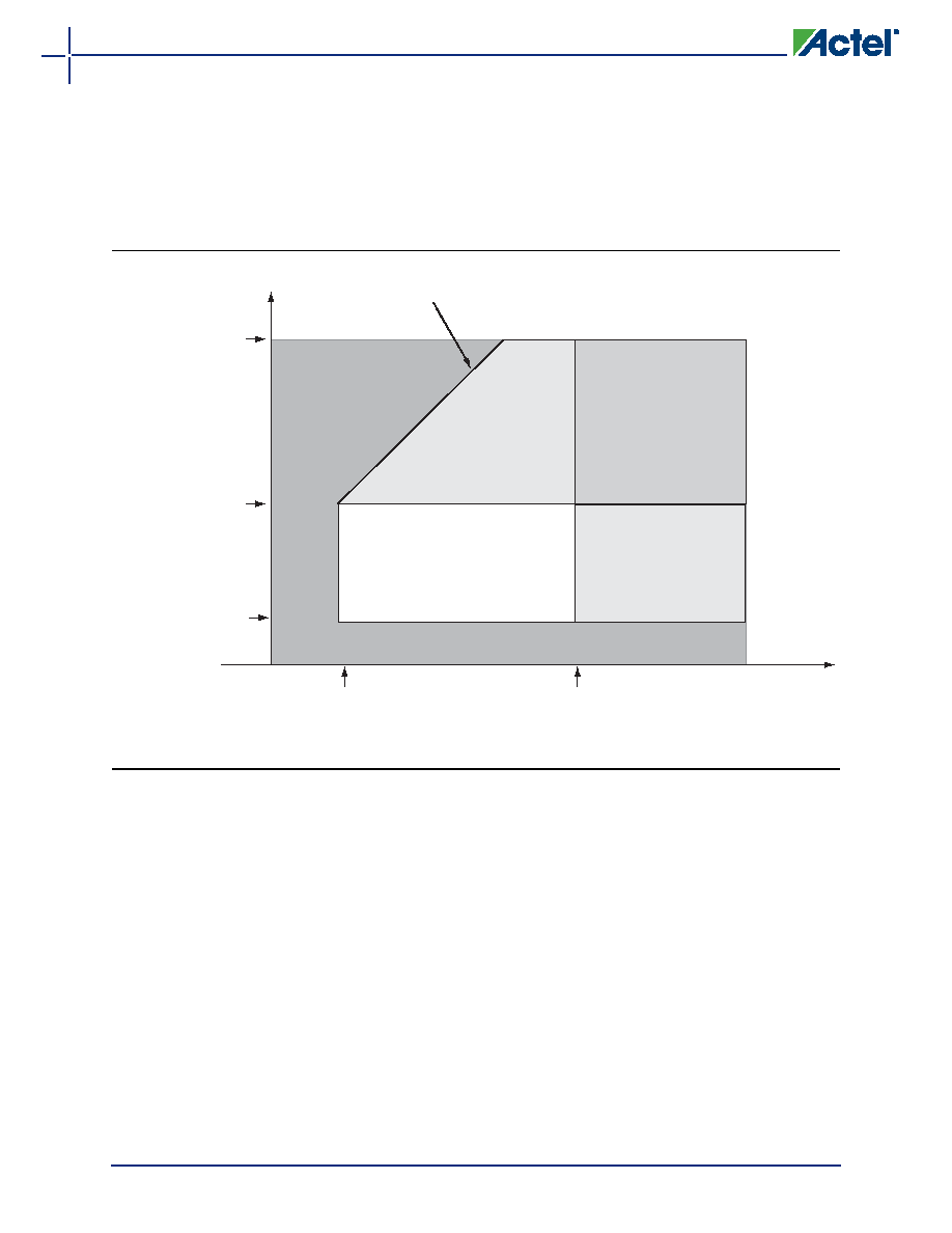
Figure 2-1 I/O State as a Function of VCCI and VCC Voltage Levels
Region 1: I/O buffers are OFF
Region 2: I/O buffers are ON.
I/Os are functional (except differential inputs)
but slower because V
CCI
/V
CC
are below
specification. For the same reason, input
buffers do not meet V
IH
/V
IL
levels, and
output buffers do not meet V
OH
/V
OL
levels.
Min V
CCI datasheet specification
voltage at a selected I/O
standard; i.e., 1.425 V or 1.7 V
or 2.3 V or 3.0 V
VCC
VCC = 1.425 V
Region 1: I/O Buffers are OFF
Activation trip point:
Va = 0.85 V ± 0.25 V
Deactivation trip point:
Vd = 0.75 V ± 0.25 V
Activation trip point:
Va = 0.9 V ± 0.3 V
Deactivation trip point:
Vd = 0.8 V ± 0.3 V
VCC = 1.575 V
Region 5: I/O buffers are ON
and power supplies are within
specification.
I/Os meet the entire datasheet
and timer specifications for
speed, V
IH
/V
IL
, V
OH
/V
OL
, etc.
Region 4: I/O
buffers are ON.
I/Os are functional
(except differential
but slower because V
CCI is
below specification. For the
same reason, input buffers do not
meet V
IH
/V
IL
levels, and output
buffers do not meet V
OH
/V
OL
levels.
Region 4: I/O
buffers are ON.
I/Os are functional
(except differential inputs)
where VT can be from 0.58 V to 0.9 V (typically 0.75 V)
VCCI
Region 3: I/O buffers are ON.
I/Os are functional; I/O DC
specifications are met,
but I/Os are slower because
the V
CC
is below specification.
V
CC = VCCI + VT
相关PDF资料 |
PDF描述 |
|---|---|
| A3P015-1QNG68 | FPGA, 384 CLBS, 15000 GATES, 350 MHz, QCC68 |
| A3P015-2QN68I | FPGA, 384 CLBS, 15000 GATES, QCC68 |
| A3P015-2QN68 | FPGA, 384 CLBS, 15000 GATES, 350 MHz, QCC68 |
| A3P015-2QNG68I | FPGA, 384 CLBS, 15000 GATES, QCC68 |
| A3P015-2QNG68 | FPGA, 384 CLBS, 15000 GATES, 350 MHz, QCC68 |
相关代理商/技术参数 |
参数描述 |
|---|---|
| A3P015-1VQ144 | 制造商:ACTEL 制造商全称:Actel Corporation 功能描述:ProASIC3 Flash Family FPGAs |
| A3P015-1VQ144ES | 制造商:ACTEL 制造商全称:Actel Corporation 功能描述:ProASIC3 Flash Family FPGAs |
| A3P015-1VQ144I | 制造商:ACTEL 制造商全称:Actel Corporation 功能描述:ProASIC3 Flash Family FPGAs |
| A3P015-1VQ144PP | 制造商:ACTEL 制造商全称:Actel Corporation 功能描述:ProASIC3 Flash Family FPGAs |
| A3P015-1VQG144 | 制造商:ACTEL 制造商全称:Actel Corporation 功能描述:ProASIC3 Flash Family FPGAs |
发布紧急采购,3分钟左右您将得到回复。