- 您现在的位置:买卖IC网 > PDF目录294843 > ACS8946 ATM/SONET/SDH SUPPORT CIRCUIT, QCC48 PDF资料下载
参数资料
| 型号: | ACS8946 |
| 元件分类: | 数字传输电路 |
| 英文描述: | ATM/SONET/SDH SUPPORT CIRCUIT, QCC48 |
| 封装: | 7 X 7 MM, QFN-48 |
| 文件页数: | 1/40页 |
| 文件大小: | 663K |
| 代理商: | ACS8946 |
当前第1页第2页第3页第4页第5页第6页第7页第8页第9页第10页第11页第12页第13页第14页第15页第16页第17页第18页第19页第20页第21页第22页第23页第24页第25页第26页第27页第28页第29页第30页第31页第32页第33页第34页第35页第36页第37页第38页第39页第40页
Revision 3/November 2006 Semtech Corp.
Page 1
www.semtech.com
ACS8946 JAM PLL
ADVANCED COMMUNICATIONS
FINAL
Jitter Attenuating, Multiplying Phase Locked Loop,
with Protection Switch, for OC-12/STM-4 and GbE
ADVANCED COMMUNICATIONS
FINAL
DATASHEET
The ACS8946 JAM PLL is a Jitter-Attenuating, Multiplying
differential Phase-Locked Loop, for generating low jitter
output clocks compliant up to SONET OC-12 and STM-4
622.08 MHz specifications. Its primary function is to
clean up clock jitter for high performance optical line
cards with OC-12 framers and serializers. It also provides
reference switching functionality for line card protection,
and frequency translation.
Typical output jitter generation is within OC-12/STM-4
specifications, at 2.8 ps rms, making it an ideal dejittering
solution for use with Semtech clock and line card parts:
ACS8510, ACS8520, ACS8522 and ACS8530. The
ACS8946 can also be used as a basic line card protection
device in some applications.
The ACS8946 JAM PLL has two differential, frequency
programmable, LVPECL reference inputs and one
differential sync input. It has four outputs, programmable
as LVPECL or CML, and frequency programmable to any
common SONET/SDH rate i.e. 19.44 MHz, 38.88 MHz,
77.76 MHz, 155.52 MHz, 311.04 MHz and 622.08 MHz.
Jitter cleaning of Gigabit Ethernet (GbE) 125 MHz and
156.25 MHz is also possible, with output frequency
multiplication up to 625.00 MHz available.
The device's operating bandwidth (and consequently the
jitter attenuation point relating to this bandwidth) is fully
configurable, and is set by external passive components.
Note...For items marked [1],[2], etc. references are given in full
in the Reference Section on page 38.
Meets rms jitter requirements of:
Telcordia GR-253[8] for OC-3 and OC-12
ITU-T G.813[4]/G.812[3] for STM-1 and STM-4 rates
rates
PLL bandwidth and jitter peaking fully adjustable—
supports PLL loop bandwidths from 2 kHz for superior
input jitter filtering
Typical jitter generation down to:
0.3 ps rms for 250 kHz to 5 MHz band for G.813,
or EN300 462, at STM-4 (OC-12) rates
2.8 ps rms for 12 kHz to 20 MHz band (against
4.02 ps rms for GR-253-CORE at OC-48 rate)
ITU, ETSI and Telcordia frequency band results shows
exceptional performance in a “Real World”
environment (low PLL bandwidth of 2 KHz and a
typical input from an ACS8525 partner IC):
0.4 ps rms for 250 kHz to 5 MHz band for G.813,
or EN300 462, at STM-4 (OC-12) rates
2.8 ps rms for 12 kHz to 20 MHz band
Tracking range ±400 ppm about a wide range of input
frequencies
Manual or automatic control of reference selection
External feedback option
LOS alarms for each input, and for selected reference
3.3 V operation, - 40 to +85°C temperature range
Small outline leadless 7 mm x 7 mm QFN48 package
Lead (Pb)-free version available (ACS8946T),
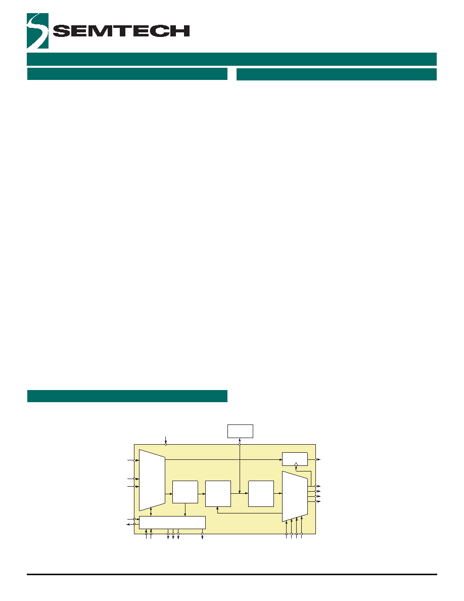
Figure 1 Simplified Block Diagram of the ACS8946 JAM PLL
Block Diagram
Introduction
Features
Loop
Filter
Re-timing
PFD
Charge
Pump
2.5 GHz
VCO
Divider
Frequency
Dividers
Clock
Drivers
Input
Selector
Control and Monitor
4 x LVPECL or CML
Output Clocks,
Independently
Programmable
from:
625.00 MHz
622.08 MHz
311.04 MHz
155.52 MHz
77.76 MHz
38.88 MHz
19.44 MHz
125 MHz
156.25 MHz
Others Ethernet rates
available using divider
SYNC_OUT
OUT[4:1]
SYNC
CLK1
CLK2
Clock Input Configuration for:
- Manual selection
- Auto Ref selection
- External feedback mode
(SEL_CLK2, AUTO_SEL)
LOS Alarms for:
- CLK1 (ALARM1_CO0)
- CLK2 (ALARM2_CO1)
- Currently selected reference (ALARMC_CO3)
Lock Alarm (LOCKB)
Input References
Programmable:
19.44 MHz to
156.25 MHz
RESETB
CFG_IN[7:0]
CFG_OUT2
Device Configuration Select:
Frequency Select
(RATE[2:1]A, RATE[2:1]B)
VC
F8946D_004Blockdiag_06
2 x LVPECL
Differential
1 x LVPECL
Differential Sync Input
1 x CMOS
Single-ended
Sync Output
Note: LOS alarm outputs are also
used for device config. select
相关PDF资料 |
PDF描述 |
|---|---|
| ACT-141223-2R | 1200 MHz - 1400 MHz RF/MICROWAVE NARROW BAND LOW POWER AMPLIFIER |
| ACT-141223-4R | 1200 MHz - 1400 MHz RF/MICROWAVE NARROW BAND LOW POWER AMPLIFIER |
| ACT-141223-4 | 1200 MHz - 1400 MHz RF/MICROWAVE NARROW BAND LOW POWER AMPLIFIER |
| ACT-141223-5 | 1200 MHz - 1400 MHz RF/MICROWAVE NARROW BAND LOW POWER AMPLIFIER |
| ACT-5261PC-133F17Q | ACT 5261 64-Bit Superscaler Microprocessor |
相关代理商/技术参数 |
参数描述 |
|---|---|
| ACS8946EVB | 制造商:SEMTECH 制造商全称:Semtech Corporation 功能描述:Jitter Attenuating, Multiplying Phase Locked Loop, with Protection Switch, for OC-12/STM-4 and GbE |
| ACS8946T | 功能描述:IC JITTER ATT MULT PLL 48-QFN RoHS:是 类别:集成电路 (IC) >> 时钟/计时 - 专用 系列:- 标准包装:1,500 系列:- 类型:时钟缓冲器/驱动器 PLL:是 主要目的:- 输入:- 输出:- 电路数:- 比率 - 输入:输出:- 差分 - 输入:输出:- 频率 - 最大:- 电源电压:3.3V 工作温度:0°C ~ 70°C 安装类型:表面贴装 封装/外壳:28-SSOP(0.209",5.30mm 宽) 供应商设备封装:28-SSOP 包装:带卷 (TR) 其它名称:93786AFT |
| ACS8947T | 功能描述:IC JITTER ATT MULT PLL 48-QFN RoHS:是 类别:集成电路 (IC) >> 时钟/计时 - 专用 系列:- 标准包装:1,500 系列:- 类型:时钟缓冲器/驱动器 PLL:是 主要目的:- 输入:- 输出:- 电路数:- 比率 - 输入:输出:- 差分 - 输入:输出:- 频率 - 最大:- 电源电压:3.3V 工作温度:0°C ~ 70°C 安装类型:表面贴装 封装/外壳:28-SSOP(0.209",5.30mm 宽) 供应商设备封装:28-SSOP 包装:带卷 (TR) 其它名称:93786AFT |
| ACS9010 | 制造商:未知厂家 制造商全称:未知厂家 功能描述:Optoelectronic |
| ACS9510/50EVB | 制造商:Semtech Corporation 功能描述: |
发布紧急采购,3分钟左右您将得到回复。