参数资料
| 型号: | AD2S1210BSTZ |
| 厂商: | Analog Devices Inc |
| 文件页数: | 25/36页 |
| 文件大小: | 0K |
| 描述: | IC CONV R/D 10-16BIT 48-LQFP |
| 标准包装: | 1 |
| 类型: | R/D 转换器 |
| 分辨率(位): | 10,12,14,16 b |
| 数据接口: | 串行,并联 |
| 电压电源: | 模拟和数字 |
| 电源电压: | 4.75 V ~ 5.25 V |
| 工作温度: | -40°C ~ 85°C |
| 安装类型: | 表面贴装 |
| 封装/外壳: | 48-LQFP |
| 供应商设备封装: | 48-LQFP(7x7) |
| 包装: | 托盘 |
| 产品目录页面: | 790 (CN2011-ZH PDF) |
| 配用: | EVAL-AD2S1210EDZ-ND - BOARD EVAL AD2S1210 |
第1页第2页第3页第4页第5页第6页第7页第8页第9页第10页第11页第12页第13页第14页第15页第16页第17页第18页第19页第20页第21页第22页第23页第24页当前第25页第26页第27页第28页第29页第30页第31页第32页第33页第34页第35页第36页
AD2S1210
Rev. A | Page 31 of 36
INCREMENTAL ENCODER OUTPUTS
The A, B, and NM incremental encoder emulation outputs are
free running and are valid if the resolver format input signals
applied to the converter are valid.
The AD2S1210 can be configured to emulate a 256-line, a
1024-line, a 4096-line, or a 16,384-line encoder. For example,
if the AD2S1210 is configured for 12-bit resolution, one revolu-
tion produces 1024 A and B pulses. Pulse A leads Pulse B for
increasing angular rotation (that is, clockwise direction).
The resolution of the encoder emulation outputs of the AD2S1210
is generally configured to match the resolution of the digital output.
However, the encoder emulation outputs of the AD2S1210 can also
be configured to have a lower resolution than the digital outputs.
For example, if the AD2S1210 is configured for 16-bit resolu-
tion, then the encoder emulation outputs can also be configured
for 14-bit, 12-bit, or 10-bit resolution. However, the resolution
of the encoder emulation outputs cannot be higher than the
resolution of the digital output. If the AD2S1210 is configured
such that the resolution of the encoder emulation outputs is
higher than the resolution of the digital outputs, the AD2S1210
internally overrides this configuration. In this event, the resolu-
tion of the encoder outputs is set to match the resolution of the
digital outputs. The resolution of the encoder emulation outputs
can be programmed by writing to Bit D3 and Bit D2 of the
control register.
The north marker pulse is generated as the absolute angular
position passes through zero. The north marker pulse width
is set internally for 90° and is defined relative to the A cycle.
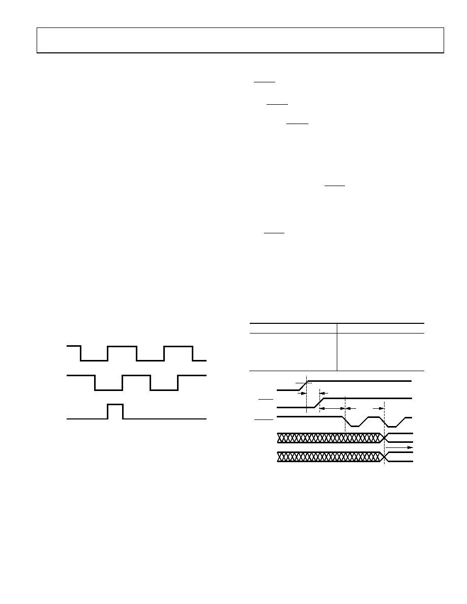
Figure 36 details the relationship between A, B, and NM.
07
46
7-
03
5
A
B
NM
Figure 36. A, B, and NM Timing for Clockwise Rotation
The inclusion of A and B outputs allows the AD2S1210 with
resolver solution to replace optical encoders directly without
the need to change or upgrade existing application software.
SUPPLY SEQUENCING AND RESET
The AD2S1210 requires an external reset signal to hold the
RESET input low until VDD is within the specified operating
range of 4.5 V to 5.5 V.
The RESET pin must be held low for a minimum of 10 μs after
VDD is within the specified range (shown as tRST in
).
Applying a
RESET signal to the AD2S1210 initializes the output
position to a value of 0x000 (degrees output through the parallel,
serial, and encoder interfaces) and causes LOS to be indicated
(LOT and DOS pins pulled low), as shown in
.
Failure to apply the correct power-up/reset sequence may result
in an incorrect position indication.
After a rising edge on the RESET input, the device must be allowed
at least tTRACK ms (see
) for the internal circuitry to stabil-
ize and the tracking loop to settle to the step change of the input
position. For the duration of tTRACK fault indications may occur
on the LOT and DOS pins due to the step response caused by
the
RESET. The duration of tTRACK is dependent on the converter
resolution as outlined in
. After tTRACK, the fault register
should be read and cleared as outlined in the
section. The time required to read and clear the fault
register is indicated as tFAULT, and is defined by the interface
speed of the DSP/microprocessor used in the application. (Note
that if position data is acquired via the encoder outputs, these
can be monitored during tTRACK.)
Table 27. tTRACK vs. Resolution (fCLKIN = 8.192 MHz)
Resolution (Bits)
tTRACK (ms)
10
12
20
14
25
16
60
VDD
DOS
LOT
SAMPLE
RESET
VALID
OUTPUT
DATA
07457-
036
tRST
tTRACK
tFAULT
4.75V
Figure 37. Power Supply Sequencing and Reset
相关PDF资料 |
PDF描述 |
|---|---|
| V110A24M300B | CONVERTER MOD DC/DC 24V 300W |
| AD7606BSTZ-6 | IC DAS W/ADC 16BIT 6CH 64LQFP |
| AD2S1210CSTZ | IC CONV R/D VAR RES OSC 48-LQFP |
| VI-24P-MY-S | CONVERTER MOD DC/DC 13.8V 50W |
| AD7607BSTZ | IC DAS W/ADC 14BIT 8CH 64LQFP |
相关代理商/技术参数 |
参数描述 |
|---|---|
| AD2S1210BSTZ-DASSAULT | 制造商:Analog Devices 功能描述: |
| AD2S1210CSTZ | 功能描述:IC CONV R/D VAR RES OSC 48-LQFP RoHS:是 类别:集成电路 (IC) >> 数据采集 - ADCs/DAC - 专用型 系列:- 产品培训模块:Lead (SnPb) Finish for COTS Obsolescence Mitigation Program 标准包装:50 系列:- 类型:数据采集系统(DAS) 分辨率(位):16 b 采样率(每秒):21.94k 数据接口:MICROWIRE?,QSPI?,串行,SPI? 电压电源:模拟和数字 电源电压:1.8 V ~ 3.6 V 工作温度:-40°C ~ 85°C 安装类型:表面贴装 封装/外壳:40-WFQFN 裸露焊盘 供应商设备封装:40-TQFN-EP(6x6) 包装:托盘 |
| AD2S1210DSTZ | 功能描述:IC CONV R/D VAR RES OSC 48LQFP RoHS:是 类别:集成电路 (IC) >> 数据采集 - ADCs/DAC - 专用型 系列:- 产品培训模块:Lead (SnPb) Finish for COTS Obsolescence Mitigation Program 标准包装:50 系列:- 类型:数据采集系统(DAS) 分辨率(位):16 b 采样率(每秒):21.94k 数据接口:MICROWIRE?,QSPI?,串行,SPI? 电压电源:模拟和数字 电源电压:1.8 V ~ 3.6 V 工作温度:-40°C ~ 85°C 安装类型:表面贴装 封装/外壳:40-WFQFN 裸露焊盘 供应商设备封装:40-TQFN-EP(6x6) 包装:托盘 |
| AD2S1210DSTZ | 制造商:Analog Devices 功能描述:IC, ADC, 16BIT, PARALLEL, SERIAL, LQFP-4 |
| AD2S1210SST-EP-RL7 | 功能描述:模数转换器 - ADC IC 10-16 Bit R/D Cnvtr w/Ref Oscilltr RoHS:否 制造商:Analog Devices 通道数量: 结构: 转换速率: 分辨率: 输入类型: 信噪比: 接口类型: 工作电源电压: 最大工作温度: 安装风格: 封装 / 箱体: |
发布紧急采购,3分钟左右您将得到回复。