参数资料
| 型号: | AD2S1210BSTZ |
| 厂商: | Analog Devices Inc |
| 文件页数: | 36/36页 |
| 文件大小: | 0K |
| 描述: | IC CONV R/D 10-16BIT 48-LQFP |
| 标准包装: | 1 |
| 类型: | R/D 转换器 |
| 分辨率(位): | 10,12,14,16 b |
| 数据接口: | 串行,并联 |
| 电压电源: | 模拟和数字 |
| 电源电压: | 4.75 V ~ 5.25 V |
| 工作温度: | -40°C ~ 85°C |
| 安装类型: | 表面贴装 |
| 封装/外壳: | 48-LQFP |
| 供应商设备封装: | 48-LQFP(7x7) |
| 包装: | 托盘 |
| 产品目录页面: | 790 (CN2011-ZH PDF) |
| 配用: | EVAL-AD2S1210EDZ-ND - BOARD EVAL AD2S1210 |
第1页第2页第3页第4页第5页第6页第7页第8页第9页第10页第11页第12页第13页第14页第15页第16页第17页第18页第19页第20页第21页第22页第23页第24页第25页第26页第27页第28页第29页第30页第31页第32页第33页第34页第35页当前第36页
AD2S1210
Rev. A | Page 9 of 36
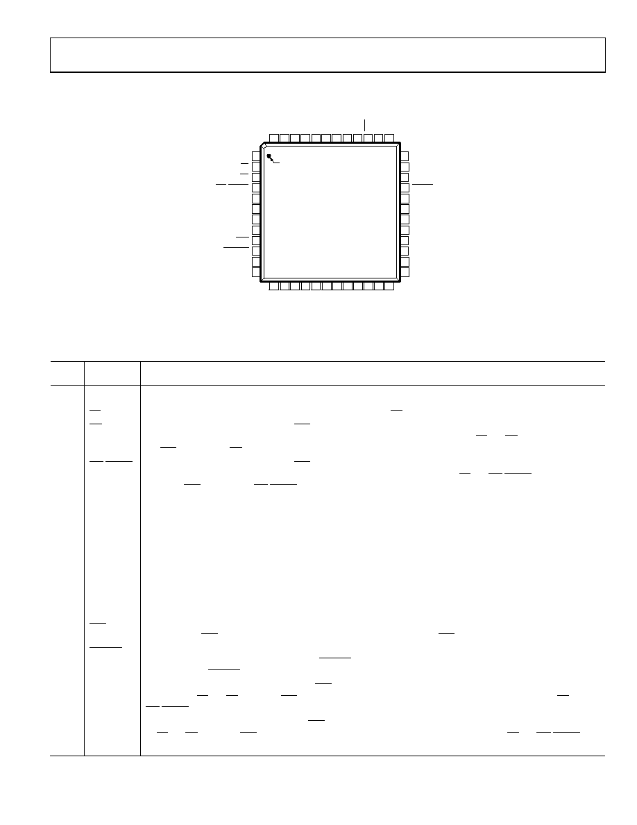
PIN CONFIGURATION AND FUNCTION DESCRIPTIONS
48
RE
S
0
47
RE
F
O
U
T
46
RE
F
BY
P
45
CO
S
44
CO
S
L
O
43
AV
DD
42
SI
N
L
O
41
SI
N
40
AG
ND
39
EX
C
38
EX
C
37
A0
35
DOS
34
LOT
33
RESET
30
B
31
NM
32
DIR
36
A1
29
A
28
DB0
27
DB1
25
DB3
26
DB2
2
CS
3
RD
4
WR/FSYNC
7
CLKIN
6
DVDD
5
DGND
1
RES1
8
XTALOUT
9
SOE
10
SAMPLE
12
DB14/SDI
11
DB15/SDO
13
DB13/
S
C
L
K
14
DB12
15
DB
11
16
DB10
17
DB9
18
V
DR
IV
E
19
DG
ND
20
DB8
21
DB7
22
DB6
23
DB5
24
DB4
PIN 1
AD2S1210
TOP VIEW
(Not to Scale)
07
46
7-
0
02
Figure 2. Pin Configuration
Table 4. Pin Function Descriptions
Pin
No.
Mnemonic
Description
1
RES1
Resolution Select 1. Logic input. RES1 in conjunction with RES0 allows the resolution of the AD2S1210 to be
programmed. Refer to the Configuration of AD2S1210 section.
2
CS
Chip Select. Active low logic input. The device is enabled when CS is held low.
3
RD
Edge-Triggered Logic Input. When the SOE pin is high, this pin acts as a frame synchronization signal and output
enable for the parallel data outputs, DB15 to DB0. The output buffer is enabled when CS and RD are held low. When
the SOE pin is low, the RD pin should be held high.
4
WR/FSYNC
Edge-Triggered Logic Input. When the SOE pin is high, this pin acts as a frame synchronization signal and input
enable for the parallel data inputs, DB7 to DB0. The input buffer is enabled when CS and WR/FSYNC are held low.
When the SOE pin is low, the WR/FSYNC pin acts as a frame synchronization signal and enable for the serial data bus.
5, 19
DGND
Digital Ground. These pins are ground reference points for digital circuitry on the AD2S1210. Refer all digital input
signals to this DGND voltage. Both of these pins can be connected to the AGND plane of a system. The DGND and
AGND voltages should ideally be at the same potential and must not be more than 0.3 V apart, even on a transient basis.
6
DVDD
Digital Supply Voltage, 4.75 V to 5.25 V. This is the supply voltage for all digital circuitry on the AD2S1210. The AVDD and DVDD
voltages ideally should be at the same potential and must not be more than 0.3 V apart, even on a transient basis.
7
CLKIN
Clock Input. A crystal or oscillator can be used at the CLKIN and XTALOUT pins to supply the required clock frequency of
the AD2S1210. Alternatively, a single-ended clock can be applied to the CLKIN pin. The input frequency of the AD2S1210 is
specified from 6.144 MHz to 10.24 MHz.
8
XTALOUT
Crystal Output. When using a crystal or oscillator to supply the clock frequency to the AD2S1210, apply the crystal
across the CLKIN and XTALOUT pins. When using a single-ended clock source, the XTALOUT pin should be
considered a no connect pin.
9
SOE
Serial Output Enable. Logic input. This pin enables either the parallel or serial interface. The serial interface is selected
by holding the SOE pin low, and the parallel interface is selected by holding the SOE pin high.
10
SAMPLE
Sample Result. Logic input. Data is transferred from the position and velocity integrators to the position and velocity
registers, after a high-to-low transition on the SAMPLE signal. The fault register is also updated after a high-to-low
transition on the SAMPLE signal.
11
DB15/SDO
Data Bit 15/Serial Data Output Bus. When the SOE pin is high, this pin acts as DB15, a three-state data output pin
controlled by CS and RD. When the SOE pin is low, this pin acts as SDO, the serial data output bus controlled by CS and
WR/FSYNC. The bits are clocked out on the rising edge of SCLK.
12
DB14/SDI
Data Bit 14/Serial Data Input Bus. When the SOE pin is high, this pin acts as DB14, a three-state data output pin controlled
by CS and RD. When the SOE pin is low, this pin acts as SDI, the serial data input bus controlled by CS and WR/FSYNC. The
bits are clocked in on the falling edge of SCLK.
相关PDF资料 |
PDF描述 |
|---|---|
| V110A24M300B | CONVERTER MOD DC/DC 24V 300W |
| AD7606BSTZ-6 | IC DAS W/ADC 16BIT 6CH 64LQFP |
| AD2S1210CSTZ | IC CONV R/D VAR RES OSC 48-LQFP |
| VI-24P-MY-S | CONVERTER MOD DC/DC 13.8V 50W |
| AD7607BSTZ | IC DAS W/ADC 14BIT 8CH 64LQFP |
相关代理商/技术参数 |
参数描述 |
|---|---|
| AD2S1210BSTZ-DASSAULT | 制造商:Analog Devices 功能描述: |
| AD2S1210CSTZ | 功能描述:IC CONV R/D VAR RES OSC 48-LQFP RoHS:是 类别:集成电路 (IC) >> 数据采集 - ADCs/DAC - 专用型 系列:- 产品培训模块:Lead (SnPb) Finish for COTS Obsolescence Mitigation Program 标准包装:50 系列:- 类型:数据采集系统(DAS) 分辨率(位):16 b 采样率(每秒):21.94k 数据接口:MICROWIRE?,QSPI?,串行,SPI? 电压电源:模拟和数字 电源电压:1.8 V ~ 3.6 V 工作温度:-40°C ~ 85°C 安装类型:表面贴装 封装/外壳:40-WFQFN 裸露焊盘 供应商设备封装:40-TQFN-EP(6x6) 包装:托盘 |
| AD2S1210DSTZ | 功能描述:IC CONV R/D VAR RES OSC 48LQFP RoHS:是 类别:集成电路 (IC) >> 数据采集 - ADCs/DAC - 专用型 系列:- 产品培训模块:Lead (SnPb) Finish for COTS Obsolescence Mitigation Program 标准包装:50 系列:- 类型:数据采集系统(DAS) 分辨率(位):16 b 采样率(每秒):21.94k 数据接口:MICROWIRE?,QSPI?,串行,SPI? 电压电源:模拟和数字 电源电压:1.8 V ~ 3.6 V 工作温度:-40°C ~ 85°C 安装类型:表面贴装 封装/外壳:40-WFQFN 裸露焊盘 供应商设备封装:40-TQFN-EP(6x6) 包装:托盘 |
| AD2S1210DSTZ | 制造商:Analog Devices 功能描述:IC, ADC, 16BIT, PARALLEL, SERIAL, LQFP-4 |
| AD2S1210SST-EP-RL7 | 功能描述:模数转换器 - ADC IC 10-16 Bit R/D Cnvtr w/Ref Oscilltr RoHS:否 制造商:Analog Devices 通道数量: 结构: 转换速率: 分辨率: 输入类型: 信噪比: 接口类型: 工作电源电压: 最大工作温度: 安装风格: 封装 / 箱体: |
发布紧急采购,3分钟左右您将得到回复。