参数资料
| 型号: | AD5315BRM |
| 厂商: | Analog Devices Inc |
| 文件页数: | 13/24页 |
| 文件大小: | 0K |
| 描述: | IC DAC 10BIT 2WIRE I2C 10-MSOP |
| 产品培训模块: | Data Converter Fundamentals DAC Architectures |
| 标准包装: | 50 |
| 设置时间: | 6µs |
| 位数: | 10 |
| 数据接口: | I²C,串行 |
| 转换器数目: | 4 |
| 电压电源: | 单电源 |
| 功率耗散(最大): | 5mW |
| 工作温度: | -40°C ~ 105°C |
| 安装类型: | 表面贴装 |
| 封装/外壳: | 10-TFSOP,10-MSOP(0.118",3.00mm 宽) |
| 供应商设备封装: | 10-MSOP |
| 包装: | 管件 |
| 输出数目和类型: | 4 电压,单极;4 电压,双极 |
| 采样率(每秒): | 143k |
AD5305/AD5315/AD5325
Rev. G | Page 20 of 24
APPLICATIONS
TYPICAL APPLICATION CIRCUIT
The AD5305/AD5315/AD5325 can be used with a wide range
of reference voltages where the devices offer full, one-quadrant
multiplying capability over a reference range of 0 V to VDD.
More typically, these devices are used with a fixed, precision
reference voltage. Suitable references for 5 V operation are the
AD780 and REF192 (2.5 V references). For 2.5 V operation, a
suitable external reference is the AD589, a 1.23 V band gap
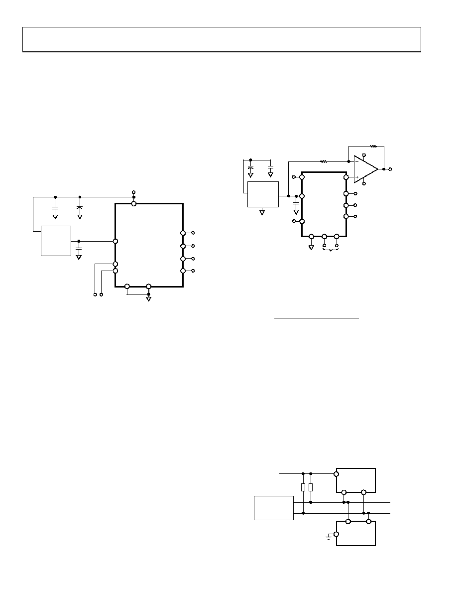
reference. Figure 36 shows a typical setup for the AD5305/
AD5315/AD5325 when using an external reference. Note that
A0 can be high or low.
GND
SDA
0.1F
REFIN
A0
10F
1F
SCL
VDD = 2.5V TO 5.5V
VIN
EXT
REF
VOUT
AD780/REF192
WITH VDD = 5V
OR AD589 WITH
VDD = 2.5V
AD5305/
AD5315/
AD5325
VOUTD
VOUTC
VOUTB
VOUTA
SERIAL
INTERFACE
00
93
0-
0
36
Figure 36. AD5305/AD5315/AD5325 Using External Reference
If an output range of 0 V to VDD is required, the simplest
solution is to connect the reference input to VDD. As this
supply may not be very accurate and may be noisy, the
AD5305/AD5315/AD5325 can be powered from the reference
voltage; for example, using a 5 V reference such as the REF195.
The REF195 outputs a steady supply voltage for the AD5305/
AD5315/AD5325. The typical current required from the
REF195 is 600 μA supply current and approximately 112 μA
into the reference input. This is with no load on the DAC
outputs. When the DAC outputs are loaded, the REF195 also
needs to supply the current to the loads. The total current
required (with a 10 kΩ load on each output) is
712 μA + 4(5 V/10 kΩ) = 2.70 mA
The load regulation of the REF195 is typically 2 ppm/mA,
which results in an error of 5.4 ppm (27 μV) for the 2.7 mA
current drawn from it. This corresponds to a 0.0014 LSB error
at eight bits and 0.022 LSB error at 12 bits.
BIPOLAR OPERATION
The AD5305/AD5315/AD5325 have been designed for single
supply operation, but a bipolar output range is also possible using
the circuit in Figure 37. This circuit gives an output voltage
range of 5 V. Rail-to-rail operation at the amplifier output is
achievable using an AD820 or an OP295 as the output amplifier.
+5V
–5V
10F
6V TO 12V
AD5305
0.1F
R1 = 10k
±5V
R2 = 10k
REFIN
A0
GND
AD1585
1F
+5V
VDD
2-WIRE
SERIAL
INTERFACE
VOUTD
VOUTC
VOUTB
VOUTA
VIN
VOUT
00
93
0-
03
7
GND SCL SDA
AD820/
OP295
Figure 37. Bipolar Operation with the AD5305
The output voltage for any input code can be calculated as
follows:
(
)
(
) ()
()
×
+
×
=
1
/
2
1
2
1
2
/
R
REFIN
R
D
REFIN
V
N
OUT
where:
D is the decimal equivalent of the code loaded to the DAC.
N is the DAC resolution.
REFIN is the reference voltage input.
with
REFIN = 5 V, R1 = R2 = 10 kΩ, VOUT (10 × D/2N) 5 V
MULTIPLE DEVICES ON ONE BUS
Figure 38 shows two AD5305 devices on the same serial bus.
Each has a different slave address because the state of the A0 pin
is different. This allows each of eight DACs to be written to or
read from independently.
SCL
SDA
AD5305
A0
AD5305
SCL
SDA
A0
MICRO-
CONTROLLER
PULL-UP
RESISTORS
VDD
00
93
0-
0
38
Figure 38. Multiple AD5305 Devices on One Bus
相关PDF资料 |
PDF描述 |
|---|---|
| IDT74FCT807CTPY | IC CLK BUFFER 1:10 100MHZ 20SSOP |
| IDT74FCT807BTSOI8 | IC CLK BUFFER 1:10 100MHZ 20SOIC |
| AD5314BRM | IC DAC 10BIT QUAD VOUT 10-MSOP |
| IDT74FCT807BTSOI | IC CLK BUFFER 1:10 100MHZ 20SOIC |
| LTC1454IS#TRPBF | IC D/A CONV 12BIT R-R DUAL16SOIC |
相关代理商/技术参数 |
参数描述 |
|---|---|
| AD5315BRM-REEL | 制造商:Analog Devices 功能描述:DAC 4-CH Resistor-String 10-bit 10-Pin MSOP T/R 制造商:Analog Devices 功能描述:DAC QUAD RES-STRING 10-BIT 10MSOP - Tape and Reel |
| AD5315BRM-REEL7 | 功能描述:IC DAC 10BIT 2WIRE I2C 10-MSOP RoHS:否 类别:集成电路 (IC) >> 数据采集 - 数模转换器 系列:- 产品培训模块:LTC263x 12-, 10-, and 8-Bit VOUT DAC Family 特色产品:LTC2636 - Octal 12-/10-/8-Bit SPI VOUT DACs with 10ppm/°C Reference 标准包装:91 系列:- 设置时间:4µs 位数:10 数据接口:MICROWIRE?,串行,SPI? 转换器数目:8 电压电源:单电源 功率耗散(最大):2.7mW 工作温度:-40°C ~ 85°C 安装类型:表面贴装 封装/外壳:14-WFDFN 裸露焊盘 供应商设备封装:14-DFN-EP(4x3) 包装:管件 输出数目和类型:8 电压,单极 采样率(每秒):* |
| AD5315BRMZ | 功能描述:IC DAC 10BIT 2WIRE I2C 10-MSOP RoHS:是 类别:集成电路 (IC) >> 数据采集 - 数模转换器 系列:- 产品培训模块:Lead (SnPb) Finish for COTS Obsolescence Mitigation Program 标准包装:50 系列:- 设置时间:4µs 位数:12 数据接口:串行 转换器数目:2 电压电源:单电源 功率耗散(最大):- 工作温度:-40°C ~ 85°C 安装类型:表面贴装 封装/外壳:8-TSSOP,8-MSOP(0.118",3.00mm 宽) 供应商设备封装:8-uMAX 包装:管件 输出数目和类型:2 电压,单极 采样率(每秒):* 产品目录页面:1398 (CN2011-ZH PDF) |
| AD5315BRMZ1 | 制造商:AD 制造商全称:Analog Devices 功能描述:2.5 V to 5.5 V, 500 ??A, 2-Wire Interface Interface |
| AD5315BRMZ-REEL | 功能描述:IC DAC 10BIT 2WIRE I2C 10MSOP RoHS:是 类别:集成电路 (IC) >> 数据采集 - 数模转换器 系列:- 产品培训模块:LTC263x 12-, 10-, and 8-Bit VOUT DAC Family 特色产品:LTC2636 - Octal 12-/10-/8-Bit SPI VOUT DACs with 10ppm/°C Reference 标准包装:91 系列:- 设置时间:4µs 位数:10 数据接口:MICROWIRE?,串行,SPI? 转换器数目:8 电压电源:单电源 功率耗散(最大):2.7mW 工作温度:-40°C ~ 85°C 安装类型:表面贴装 封装/外壳:14-WFDFN 裸露焊盘 供应商设备封装:14-DFN-EP(4x3) 包装:管件 输出数目和类型:8 电压,单极 采样率(每秒):* |
发布紧急采购,3分钟左右您将得到回复。