参数资料
| 型号: | AD5315BRM |
| 厂商: | Analog Devices Inc |
| 文件页数: | 7/24页 |
| 文件大小: | 0K |
| 描述: | IC DAC 10BIT 2WIRE I2C 10-MSOP |
| 产品培训模块: | Data Converter Fundamentals DAC Architectures |
| 标准包装: | 50 |
| 设置时间: | 6µs |
| 位数: | 10 |
| 数据接口: | I²C,串行 |
| 转换器数目: | 4 |
| 电压电源: | 单电源 |
| 功率耗散(最大): | 5mW |
| 工作温度: | -40°C ~ 105°C |
| 安装类型: | 表面贴装 |
| 封装/外壳: | 10-TFSOP,10-MSOP(0.118",3.00mm 宽) |
| 供应商设备封装: | 10-MSOP |
| 包装: | 管件 |
| 输出数目和类型: | 4 电压,单极;4 电压,双极 |
| 采样率(每秒): | 143k |
AD5305/AD5315/AD5325
Rev. G | Page 15 of 24
FUNCTIONAL DESCRIPTION
The AD5305/AD5315/AD5325 are quad resistor-string DACs
fabricated on a CMOS process with resolutions of 8, 10, and 12
bits, respectively. Each contains four output buffer amplifiers
and is written to via a 2-wire serial interface. They operate from
single supplies of 2.5 V to 5.5 V, and the output buffer amplifiers
provide rail-to-rail output swing with a slew rate of 0.7 V/μs.
The four DACs share a single reference input pin. The devices
have three programmable power-down modes, in which all
DACs can be turned off completely with a high impedance
output, or the outputs can be pulled low by on-chip resistors.
DIGITAL-TO-ANALOG SECTION
The architecture of one DAC channel consists of a resistor-
string DAC followed by an output buffer amplifier. The voltage
at the REFIN pin provides the reference voltage for the DAC.
Figure 29 shows a block diagram of the DAC architecture.
Because the input coding to the DAC is straight binary, the ideal
output voltage is given by
N
REF
OUT
D
V
2
×
=
where:
D = decimal equivalent of the binary code, which is loaded to
the DAC register:
0 to 255 for AD5305 (8 bits)
0 to 1023 for AD5315 (10 bits)
0 to 4095 for AD5325 (12 bits)
N = DAC resolution
REFIN
INPUT
REGISTER
DAC
REGISTER
RESISTOR
STRING
OUTPUT BUFFER
AMPLIFIER
VOUTA
0
09
30-
02
9
Figure 29. DAC Channel Architecture
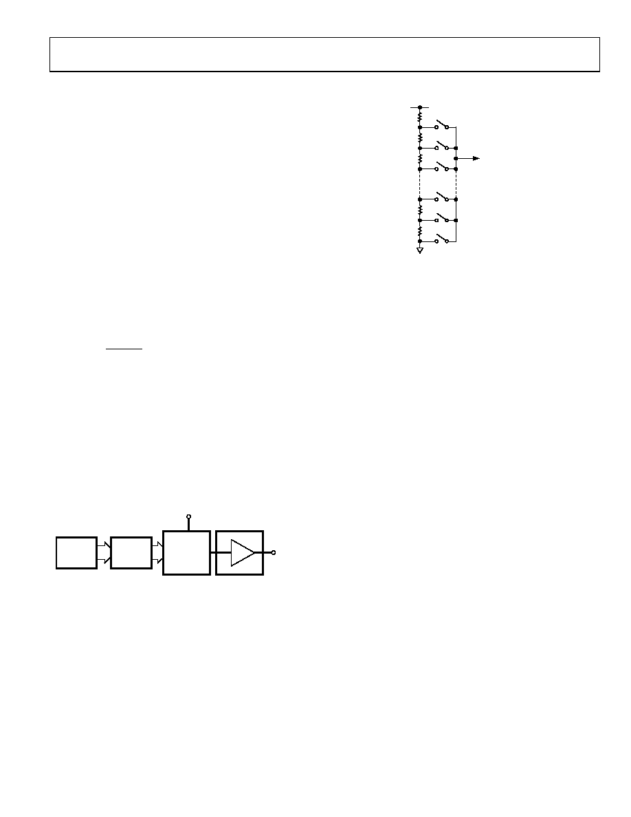
RESISTOR STRING
The resistor string section is shown in Figure 30. It is simply a
string of resistors, each of value R. The digital code loaded to
the DAC register determines at what node on the string the
voltage is tapped off to be fed into the output amplifier. The
voltage is tapped off by closing one of the switches connecting
the string to the amplifier. Because it is a string of resistors, it is
guaranteed monotonic.
R
TO OUTPUT
AMPLIFIER
00
93
0-
0
30
Figure 30. Resistor String
DAC REFERENCE INPUTS
There is a single reference input pin for the four DACs. The
reference input is unbuffered. The user can have a reference
voltage as low as 0.25 V and as high as VDD because there is no
restriction due to headroom and footroom of any reference
amplifier.
It is recommended to use a buffered reference in the external
circuit (for example, REF192). The input impedance is typically
45 kΩ.
OUTPUT AMPLIFIER
The output buffer amplifier is capable of generating rail-to-rail
voltages on its output, which gives an output range of 0 V to
VDD when the reference is VDD. It is capable of driving a load of
2 kΩ to GND or VDD, in parallel with 500 pF to GND or VDD.
The source and sink capabilities of the output amplifier can be
seen in the plot in Figure 14.
The slew rate is 0.7 V/μs with a half-scale settling time to
±0.5 LSB (at eight bits) of 6 μs.
POWER-ON RESET
The AD5305/AD5315/AD5325 are provided with a power-on
reset function, so that they power up in a defined state. The
power-on state is
Normal operation
Output voltage set to 0 V
Both input and DAC registers are filled with zeros and remain
so until a valid write sequence is made to the device. This is
particularly useful in applications where it is important to know
the state of the DAC outputs while the device is powering up.
相关PDF资料 |
PDF描述 |
|---|---|
| IDT74FCT807CTPY | IC CLK BUFFER 1:10 100MHZ 20SSOP |
| IDT74FCT807BTSOI8 | IC CLK BUFFER 1:10 100MHZ 20SOIC |
| AD5314BRM | IC DAC 10BIT QUAD VOUT 10-MSOP |
| IDT74FCT807BTSOI | IC CLK BUFFER 1:10 100MHZ 20SOIC |
| LTC1454IS#TRPBF | IC D/A CONV 12BIT R-R DUAL16SOIC |
相关代理商/技术参数 |
参数描述 |
|---|---|
| AD5315BRM-REEL | 制造商:Analog Devices 功能描述:DAC 4-CH Resistor-String 10-bit 10-Pin MSOP T/R 制造商:Analog Devices 功能描述:DAC QUAD RES-STRING 10-BIT 10MSOP - Tape and Reel |
| AD5315BRM-REEL7 | 功能描述:IC DAC 10BIT 2WIRE I2C 10-MSOP RoHS:否 类别:集成电路 (IC) >> 数据采集 - 数模转换器 系列:- 产品培训模块:LTC263x 12-, 10-, and 8-Bit VOUT DAC Family 特色产品:LTC2636 - Octal 12-/10-/8-Bit SPI VOUT DACs with 10ppm/°C Reference 标准包装:91 系列:- 设置时间:4µs 位数:10 数据接口:MICROWIRE?,串行,SPI? 转换器数目:8 电压电源:单电源 功率耗散(最大):2.7mW 工作温度:-40°C ~ 85°C 安装类型:表面贴装 封装/外壳:14-WFDFN 裸露焊盘 供应商设备封装:14-DFN-EP(4x3) 包装:管件 输出数目和类型:8 电压,单极 采样率(每秒):* |
| AD5315BRMZ | 功能描述:IC DAC 10BIT 2WIRE I2C 10-MSOP RoHS:是 类别:集成电路 (IC) >> 数据采集 - 数模转换器 系列:- 产品培训模块:Lead (SnPb) Finish for COTS Obsolescence Mitigation Program 标准包装:50 系列:- 设置时间:4µs 位数:12 数据接口:串行 转换器数目:2 电压电源:单电源 功率耗散(最大):- 工作温度:-40°C ~ 85°C 安装类型:表面贴装 封装/外壳:8-TSSOP,8-MSOP(0.118",3.00mm 宽) 供应商设备封装:8-uMAX 包装:管件 输出数目和类型:2 电压,单极 采样率(每秒):* 产品目录页面:1398 (CN2011-ZH PDF) |
| AD5315BRMZ1 | 制造商:AD 制造商全称:Analog Devices 功能描述:2.5 V to 5.5 V, 500 ??A, 2-Wire Interface Interface |
| AD5315BRMZ-REEL | 功能描述:IC DAC 10BIT 2WIRE I2C 10MSOP RoHS:是 类别:集成电路 (IC) >> 数据采集 - 数模转换器 系列:- 产品培训模块:LTC263x 12-, 10-, and 8-Bit VOUT DAC Family 特色产品:LTC2636 - Octal 12-/10-/8-Bit SPI VOUT DACs with 10ppm/°C Reference 标准包装:91 系列:- 设置时间:4µs 位数:10 数据接口:MICROWIRE?,串行,SPI? 转换器数目:8 电压电源:单电源 功率耗散(最大):2.7mW 工作温度:-40°C ~ 85°C 安装类型:表面贴装 封装/外壳:14-WFDFN 裸露焊盘 供应商设备封装:14-DFN-EP(4x3) 包装:管件 输出数目和类型:8 电压,单极 采样率(每秒):* |
发布紧急采购,3分钟左右您将得到回复。