参数资料
| 型号: | AD5315BRM |
| 厂商: | Analog Devices Inc |
| 文件页数: | 9/24页 |
| 文件大小: | 0K |
| 描述: | IC DAC 10BIT 2WIRE I2C 10-MSOP |
| 产品培训模块: | Data Converter Fundamentals DAC Architectures |
| 标准包装: | 50 |
| 设置时间: | 6µs |
| 位数: | 10 |
| 数据接口: | I²C,串行 |
| 转换器数目: | 4 |
| 电压电源: | 单电源 |
| 功率耗散(最大): | 5mW |
| 工作温度: | -40°C ~ 105°C |
| 安装类型: | 表面贴装 |
| 封装/外壳: | 10-TFSOP,10-MSOP(0.118",3.00mm 宽) |
| 供应商设备封装: | 10-MSOP |
| 包装: | 管件 |
| 输出数目和类型: | 4 电压,单极;4 电压,双极 |
| 采样率(每秒): | 143k |
AD5305/AD5315/AD5325
Rev. G | Page 17 of 24
Table 7. CLR and LDAC Bit Descriptions
Bit
Description
CLR
[0] All DAC registers and input registers are filled with 0s
on completion of the write sequence.
[1] Normal operation.
LDAC
[0] All four DAC registers and, therefore, all DAC outputs,
are simultaneously updated on completion of the write
sequence.
[1] Only addressed input register is updated. There is no
change in the contents of the DAC registers.
DEFAULT READBACK CONDITION
All pointer byte bits power up to 0. Therefore, if the user
initiates a readback without writing to the pointer byte first, no
single DAC channel has been specified. In this case, the default
readback bits are all 0, except for the CLR bit, which is a 1.
MULTIPLE-DAC WRITE SEQUENCE
Because there are individual bits in the pointer byte for each
DAC, it is possible to simultaneously write the same data and
control bits to 2, 3, or 4 DACs by setting the relevant bits to 1.
MULTIPLE-DAC READBACK SEQUENCE
If the user attempts to read back data from more than one DAC
at a time, the part reads back the default, power-on reset
conditions, that is, all 0s except for CLR, which is 1.
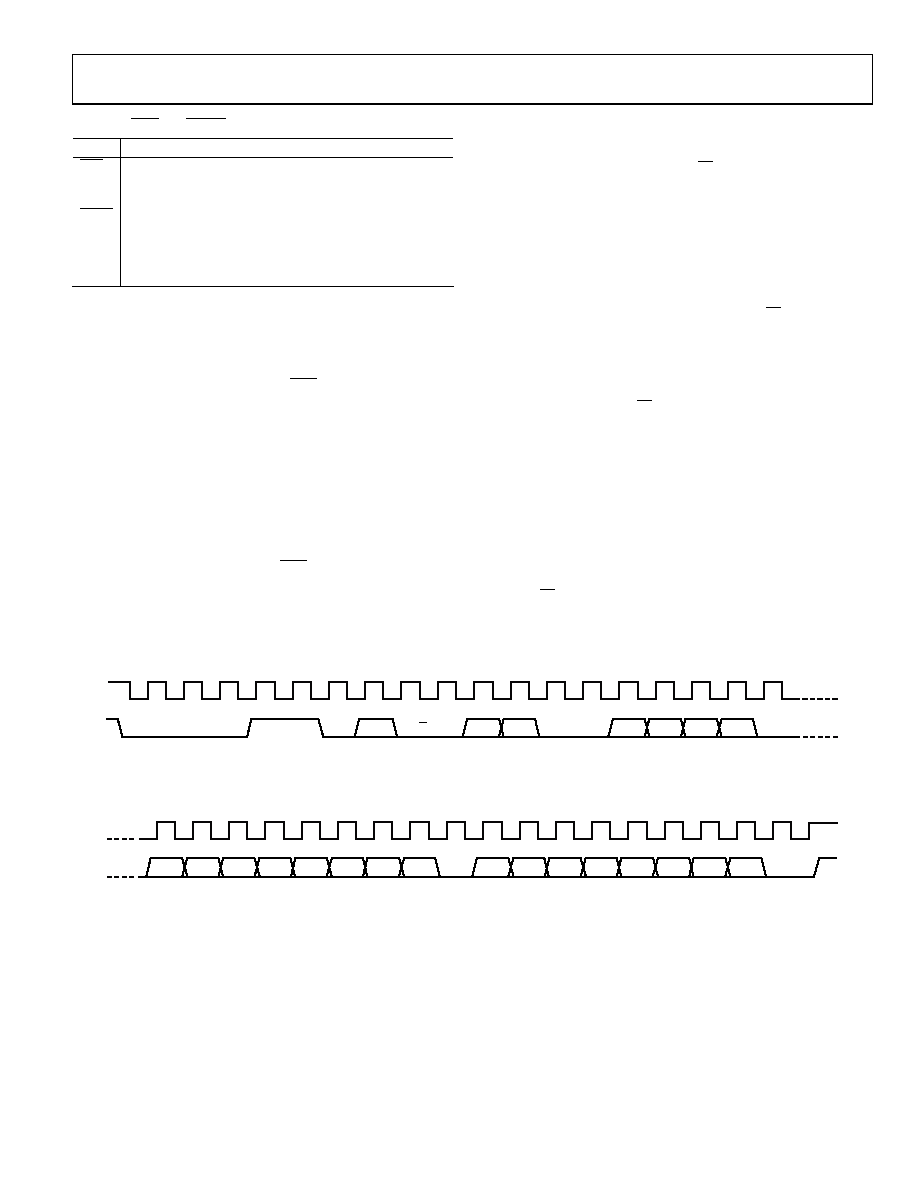
WRITE OPERATION
When writing to the AD5305/AD5315/AD5325 DACs, the user
must begin with an address byte (R/W = 0), after which the DAC
acknowledges that it is prepared to receive data by pulling SDA
low. This address byte is followed by the pointer byte, which is
also acknowledged by the DAC. Two bytes of data are then written
to the DAC, as shown in Figure 33. A stop condition follows.
READ OPERATION
When reading data back from the AD5305/AD5315/AD5325
DACs, the user begins with an address byte (R/W = 0), after
which the DAC acknowledges that it is prepared to receive data
by pulling SDA low. This address byte is usually followed by the
pointer byte, which is also acknowledged by the DAC. Following
this, there is a repeated start condition by the master and the
address is resent with R/W = 1. This is acknowledged by the
DAC indicating that it is prepared to transmit data. Two bytes
of data are then read from the DAC, as shown in Figure 34. A
stop condition follows.
However, if the master sends an ACK and continues clocking
SCL (no STOP is sent), the DAC retransmits the same two bytes
of data on SDA. This allows continuous readback of data from
the selected DAC register.
Alternatively, the user can send a start followed by the address
with R/W = 1. In this case, the previously loaded pointer settings
are used and readback of data can commence immediately.
ADDRESS BYTE
SCL
SDA
SCL
SDA
POINTER BYTE
LEAST SIGNIFICANT DATA BYTE
ACK
BY
AD53x5
MOST SIGNIFICANT DATA BYTE
MSB
LSB
MSB
LSB
STOP
COND
BY
MASTER
ACK
BY
AD53x5
ACK
BY
AD53x5
START
COND
BY
MASTER
ACK
BY
AD53x5
MSB
LSB
0
1
0
A0
R/W
X
0
093
0-
0
33
Figure 33. Write Sequence
相关PDF资料 |
PDF描述 |
|---|---|
| IDT74FCT807CTPY | IC CLK BUFFER 1:10 100MHZ 20SSOP |
| IDT74FCT807BTSOI8 | IC CLK BUFFER 1:10 100MHZ 20SOIC |
| AD5314BRM | IC DAC 10BIT QUAD VOUT 10-MSOP |
| IDT74FCT807BTSOI | IC CLK BUFFER 1:10 100MHZ 20SOIC |
| LTC1454IS#TRPBF | IC D/A CONV 12BIT R-R DUAL16SOIC |
相关代理商/技术参数 |
参数描述 |
|---|---|
| AD5315BRM-REEL | 制造商:Analog Devices 功能描述:DAC 4-CH Resistor-String 10-bit 10-Pin MSOP T/R 制造商:Analog Devices 功能描述:DAC QUAD RES-STRING 10-BIT 10MSOP - Tape and Reel |
| AD5315BRM-REEL7 | 功能描述:IC DAC 10BIT 2WIRE I2C 10-MSOP RoHS:否 类别:集成电路 (IC) >> 数据采集 - 数模转换器 系列:- 产品培训模块:LTC263x 12-, 10-, and 8-Bit VOUT DAC Family 特色产品:LTC2636 - Octal 12-/10-/8-Bit SPI VOUT DACs with 10ppm/°C Reference 标准包装:91 系列:- 设置时间:4µs 位数:10 数据接口:MICROWIRE?,串行,SPI? 转换器数目:8 电压电源:单电源 功率耗散(最大):2.7mW 工作温度:-40°C ~ 85°C 安装类型:表面贴装 封装/外壳:14-WFDFN 裸露焊盘 供应商设备封装:14-DFN-EP(4x3) 包装:管件 输出数目和类型:8 电压,单极 采样率(每秒):* |
| AD5315BRMZ | 功能描述:IC DAC 10BIT 2WIRE I2C 10-MSOP RoHS:是 类别:集成电路 (IC) >> 数据采集 - 数模转换器 系列:- 产品培训模块:Lead (SnPb) Finish for COTS Obsolescence Mitigation Program 标准包装:50 系列:- 设置时间:4µs 位数:12 数据接口:串行 转换器数目:2 电压电源:单电源 功率耗散(最大):- 工作温度:-40°C ~ 85°C 安装类型:表面贴装 封装/外壳:8-TSSOP,8-MSOP(0.118",3.00mm 宽) 供应商设备封装:8-uMAX 包装:管件 输出数目和类型:2 电压,单极 采样率(每秒):* 产品目录页面:1398 (CN2011-ZH PDF) |
| AD5315BRMZ1 | 制造商:AD 制造商全称:Analog Devices 功能描述:2.5 V to 5.5 V, 500 ??A, 2-Wire Interface Interface |
| AD5315BRMZ-REEL | 功能描述:IC DAC 10BIT 2WIRE I2C 10MSOP RoHS:是 类别:集成电路 (IC) >> 数据采集 - 数模转换器 系列:- 产品培训模块:LTC263x 12-, 10-, and 8-Bit VOUT DAC Family 特色产品:LTC2636 - Octal 12-/10-/8-Bit SPI VOUT DACs with 10ppm/°C Reference 标准包装:91 系列:- 设置时间:4µs 位数:10 数据接口:MICROWIRE?,串行,SPI? 转换器数目:8 电压电源:单电源 功率耗散(最大):2.7mW 工作温度:-40°C ~ 85°C 安装类型:表面贴装 封装/外壳:14-WFDFN 裸露焊盘 供应商设备封装:14-DFN-EP(4x3) 包装:管件 输出数目和类型:8 电压,单极 采样率(每秒):* |
发布紧急采购,3分钟左右您将得到回复。