参数资料
| 型号: | AD5315BRM |
| 厂商: | Analog Devices Inc |
| 文件页数: | 8/24页 |
| 文件大小: | 0K |
| 描述: | IC DAC 10BIT 2WIRE I2C 10-MSOP |
| 产品培训模块: | Data Converter Fundamentals DAC Architectures |
| 标准包装: | 50 |
| 设置时间: | 6µs |
| 位数: | 10 |
| 数据接口: | I²C,串行 |
| 转换器数目: | 4 |
| 电压电源: | 单电源 |
| 功率耗散(最大): | 5mW |
| 工作温度: | -40°C ~ 105°C |
| 安装类型: | 表面贴装 |
| 封装/外壳: | 10-TFSOP,10-MSOP(0.118",3.00mm 宽) |
| 供应商设备封装: | 10-MSOP |
| 包装: | 管件 |
| 输出数目和类型: | 4 电压,单极;4 电压,双极 |
| 采样率(每秒): | 143k |
AD5305/AD5315/AD5325
Rev. G | Page 16 of 24
SERIAL INTERFACE
The AD5305/AD5315/AD5325 are controlled via an I2C
compatible serial bus. The DACs are connected to this bus as
slave devices (that is, no clock is generated by the AD5305/
AD5315/AD5325 DACs). This interface is SMBus compatible
at VDD < 3.6 V.
The AD5305/AD5315/AD5325 have a 7-bit slave address. The
6 MSB are 000110 and the LSB is determined by the state of the
A0 pin. The facility to make hardwired changes to A0 allows the
user to use up to two of these devices on one bus. The 2-wire
serial bus protocol operates as follows:
1.
The master initiates data transfer by establishing a start
condition, which is when a high-to-low transition on the
SDA line occurs while SCL is high. The following byte is
the address byte, which consists of the 7-bit slave address
followed by an R/W bit (this bit determines whether data is
read from or written to the slave device).
The slave whose address corresponds to the transmitted
address responds by pulling SDA low during the ninth
clock pulse (this is termed the acknowledge bit). At this
stage, all other devices on the bus remain idle while the
selected device waits for data to be written to or read from
its shift register.
2.
Data is transmitted over the serial bus in sequences of nine
clock pulses (eight data bits followed by an acknowledge
bit). The transitions on the SDA line must occur during the
low period of SCL and remain stable during the high
period of SCL.
3.
When all data bits have been read or written, a stop
condition is established. In write mode, the master pulls
the SDA line high during the 10th clock pulse to establish a
stop condition. In read mode, the master issues a No
Acknowledge for the ninth clock pulse (that is, the SDA
line remains high). The master then brings the SDA line
low before the 10th clock pulse and then high during the
10th clock pulse to establish a stop condition.
READ/WRITE SEQUENCE
In the case of the AD5305/AD5315/AD5325, all write access
sequences and most read sequences begin with the device
address (with R/W = 0) followed by the pointer byte. This
pointer byte specifies the data format and determines which
DAC is being accessed in the subsequent read/write operation
(see Figure 31). In a write operation, the data follows
immediately. In a read operation, the address is resent with
R/W = 1 and then the data is read back. However, it is also
possible to perform a read operation by sending only the
address with R/W = 1. The previously loaded pointer settings
are then used for the readback operation. See Figure 32 for a
graphical explanation of the interface.
DACD
X
LSB
MSB
0
DACC DACB DACA
0
930-
03
1
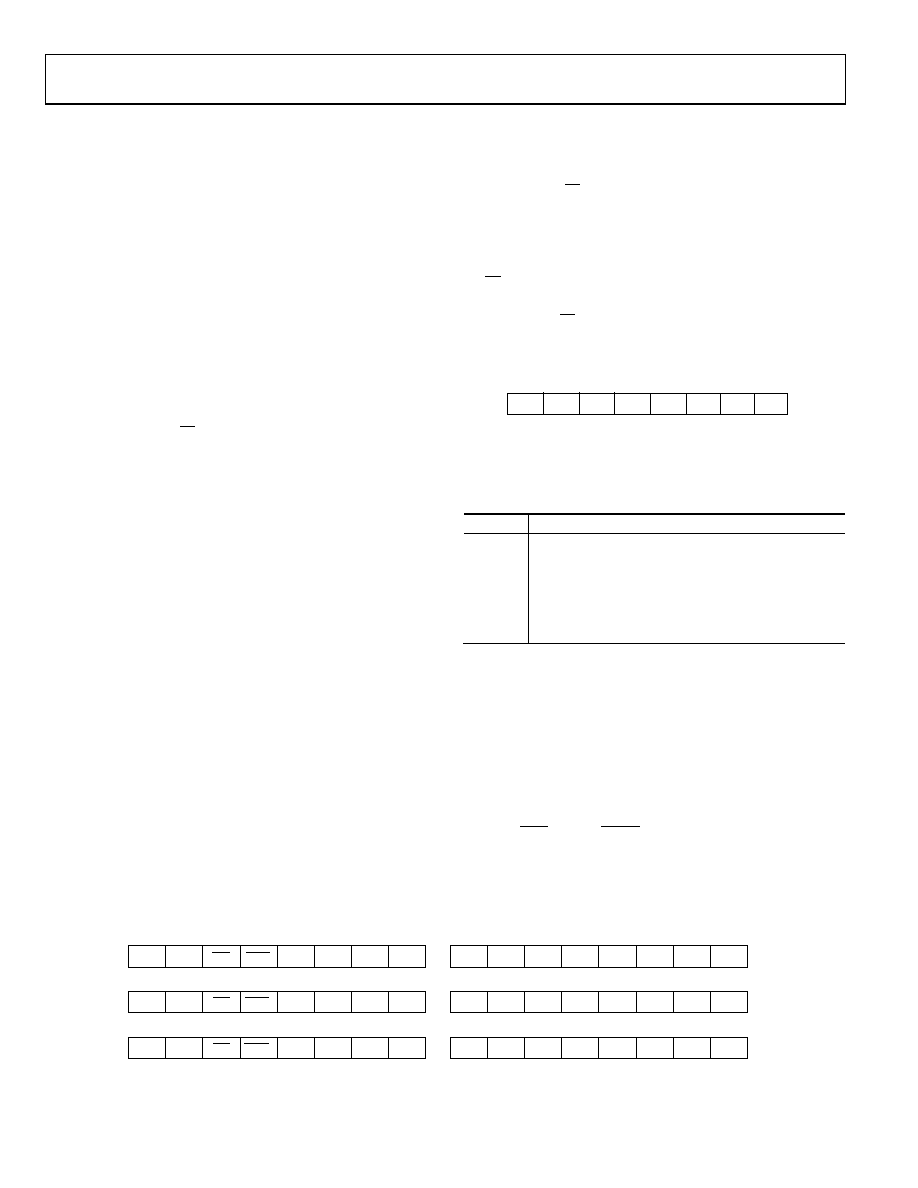
Figure 31. Pointer Byte
POINTER BYTE BITS
Table 6 explains the individual bits that make up the pointer byte.
Table 6. Individual Bits of the Pointer Byte
Bit
Description
X
Don’t care bits.
0
Reserved bits. Must be set to 0.
DACD
[1] The following data bytes are for DAC D.
DACC
[1] The following data bytes are for DAC C.
DACB
[1] The following data bytes are for DAC B.
DACA
[1] The following data bytes are for DAC A.
INPUT SHIFT REGISTER
The input shift register is 16 bits wide. Data is loaded into the
device as two data bytes on the serial data line, SDA, under the
control of the serial clock input, SCL. The timing diagram for
this operation is shown in Figure 2. The two data bytes consist
of four control bits followed by 8, 10, or 12 bits of DAC data,
depending on the device type. The first two bits loaded are the
PD1 and PD0 bits that control the mode of operation of the device.
See the Power-Down Modes section for a complete description.
Bit 13 is CLR, Bit 12 is LDAC, and the remaining bits are left
justified DAC data bits, starting with the MSB. See Figure 32.
DATA BYTES (WRITE AND READBACK)
MOST SIGNIFICANT DATA BYTE
PD0
PD1
LSB
PD0
CLR
LDAC
PD1
LSB
MSB
10-BIT AD5315
LSB
MSB
12-BIT AD5325
CLR
LDAC
MSB
8-BIT AD5305
CLR
LDAC
D7
D6
D5
D4
D9
D8
D7
D6
PD0
D11
D10
D9
D8
LEAST SIGNIFICANT DATA BYTE
LSB
MSB
10-BIT AD5315
LSB
MSB
12-BIT AD5325
MSB
8-BIT AD5305
D2
D3
D1
D0
0
D4
D5
D3
D2
D1
D0
0
D6
D7
D5
D4
D3
D2
D1
D0
0
093
0-
032
Figure 32. Data Formats for Write and Readback
相关PDF资料 |
PDF描述 |
|---|---|
| IDT74FCT807CTPY | IC CLK BUFFER 1:10 100MHZ 20SSOP |
| IDT74FCT807BTSOI8 | IC CLK BUFFER 1:10 100MHZ 20SOIC |
| AD5314BRM | IC DAC 10BIT QUAD VOUT 10-MSOP |
| IDT74FCT807BTSOI | IC CLK BUFFER 1:10 100MHZ 20SOIC |
| LTC1454IS#TRPBF | IC D/A CONV 12BIT R-R DUAL16SOIC |
相关代理商/技术参数 |
参数描述 |
|---|---|
| AD5315BRM-REEL | 制造商:Analog Devices 功能描述:DAC 4-CH Resistor-String 10-bit 10-Pin MSOP T/R 制造商:Analog Devices 功能描述:DAC QUAD RES-STRING 10-BIT 10MSOP - Tape and Reel |
| AD5315BRM-REEL7 | 功能描述:IC DAC 10BIT 2WIRE I2C 10-MSOP RoHS:否 类别:集成电路 (IC) >> 数据采集 - 数模转换器 系列:- 产品培训模块:LTC263x 12-, 10-, and 8-Bit VOUT DAC Family 特色产品:LTC2636 - Octal 12-/10-/8-Bit SPI VOUT DACs with 10ppm/°C Reference 标准包装:91 系列:- 设置时间:4µs 位数:10 数据接口:MICROWIRE?,串行,SPI? 转换器数目:8 电压电源:单电源 功率耗散(最大):2.7mW 工作温度:-40°C ~ 85°C 安装类型:表面贴装 封装/外壳:14-WFDFN 裸露焊盘 供应商设备封装:14-DFN-EP(4x3) 包装:管件 输出数目和类型:8 电压,单极 采样率(每秒):* |
| AD5315BRMZ | 功能描述:IC DAC 10BIT 2WIRE I2C 10-MSOP RoHS:是 类别:集成电路 (IC) >> 数据采集 - 数模转换器 系列:- 产品培训模块:Lead (SnPb) Finish for COTS Obsolescence Mitigation Program 标准包装:50 系列:- 设置时间:4µs 位数:12 数据接口:串行 转换器数目:2 电压电源:单电源 功率耗散(最大):- 工作温度:-40°C ~ 85°C 安装类型:表面贴装 封装/外壳:8-TSSOP,8-MSOP(0.118",3.00mm 宽) 供应商设备封装:8-uMAX 包装:管件 输出数目和类型:2 电压,单极 采样率(每秒):* 产品目录页面:1398 (CN2011-ZH PDF) |
| AD5315BRMZ1 | 制造商:AD 制造商全称:Analog Devices 功能描述:2.5 V to 5.5 V, 500 ??A, 2-Wire Interface Interface |
| AD5315BRMZ-REEL | 功能描述:IC DAC 10BIT 2WIRE I2C 10MSOP RoHS:是 类别:集成电路 (IC) >> 数据采集 - 数模转换器 系列:- 产品培训模块:LTC263x 12-, 10-, and 8-Bit VOUT DAC Family 特色产品:LTC2636 - Octal 12-/10-/8-Bit SPI VOUT DACs with 10ppm/°C Reference 标准包装:91 系列:- 设置时间:4µs 位数:10 数据接口:MICROWIRE?,串行,SPI? 转换器数目:8 电压电源:单电源 功率耗散(最大):2.7mW 工作温度:-40°C ~ 85°C 安装类型:表面贴装 封装/外壳:14-WFDFN 裸露焊盘 供应商设备封装:14-DFN-EP(4x3) 包装:管件 输出数目和类型:8 电压,单极 采样率(每秒):* |
发布紧急采购,3分钟左右您将得到回复。