参数资料
| 型号: | AD5372BSTZ |
| 厂商: | Analog Devices Inc |
| 文件页数: | 15/29页 |
| 文件大小: | 0K |
| 描述: | IC DAC 16BIT 32CH SER 64-LQFP |
| 产品培训模块: | Data Converter Fundamentals DAC Architectures |
| 标准包装: | 1 |
| 设置时间: | 20µs |
| 位数: | 16 |
| 数据接口: | 串行 |
| 转换器数目: | 32 |
| 电压电源: | 双 ± |
| 功率耗散(最大): | 520mW |
| 工作温度: | -40°C ~ 85°C |
| 安装类型: | 表面贴装 |
| 封装/外壳: | 64-LQFP |
| 供应商设备封装: | 64-LQFP(10x10) |
| 包装: | 托盘 |
| 输出数目和类型: | 32 电压,单极;32 电压,双极 |
| 采样率(每秒): | * |
| 产品目录页面: | 782 (CN2011-ZH PDF) |
| 配用: | EVAL-AD5372EBZ-ND - BOARD EVAL FOR AD5372 |
第1页第2页第3页第4页第5页第6页第7页第8页第9页第10页第11页第12页第13页第14页当前第15页第16页第17页第18页第19页第20页第21页第22页第23页第24页第25页第26页第27页第28页第29页
AD5372/AD5373
Rev. C | Page 21 of 28
SERIAL INTERFACE
The AD5372/AD5373 contain a high speed SPI operating at
clock frequencies up to 50 MHz (20 MHz for read operations).
To minimize both the power consumption of the device and
on-chip digital noise, the interface powers up fully only when
the device is being written to, that is, on the falling edge of
SYNC. The serial interface is 2.5 V LVTTL-compatible when
operating from a 2.5 V to 3.6 V DVCC supply. It is controlled by
four pins: SYNC (frame synchronization input), SDI (serial
data input pin), SCLK (clocks data in and out of the device),
and SDO (serial data output pin for data readback).
SPI WRITE MODE
The AD5372/AD5373 allow writing of data via the serial interface
to every register directly accessible to the serial interface, that is,
all registers except the X2A, X2B, and DAC registers. The X2A
and X2B registers are updated when writing to the X1A, X1B,
M, and C registers, and the DAC data registers are updated by
LDAC. The serial word (see
or
) is 24 bits long:
16 (AD5372) or 14 (AD5373) of these bits are data bits; six bits
are address bits; and two bits are mode bits that determine what
is done with the data. Two bits are reserved on the AD5373.
The serial interface works with both a continuous and a burst
(gated) serial clock. Serial data applied to SDI is clocked into
the AD5372/AD5373 by clock pulses applied to SCLK. The first
falling edge of SYNC starts the write cycle. At least 24 falling
clock edges must be applied to SCLK to clock in 24 bits of data
before SYNC is taken high again. If SYNC is taken high before
the 24th falling clock edge, the write operation is aborted.
If a continuous clock is used, SYNC must be taken high before the
25th falling clock edge. This inhibits the clock within the AD5372/
AD5373. If more than 24 falling clock edges are applied before
SYNC is taken high again, the input data becomes corrupted. If
an externally gated clock of exactly 24 pulses is used, SYNC can
be taken high any time after the 24th falling clock edge.
The input register addressed is updated on the rising edge of
SYNC. For another serial transfer to take place, SYNC must be
taken low again.
SPI READBACK MODE
The AD5372/AD5373 allow data readback via the serial
interface from every register directly accessible to the serial
interface, that is, all registers except the X2A, X2B, and DAC
data registers. To read back a register, it is first necessary to tell
the AD5372/AD5373 which register is to be read. This is achieved
by writing a word whose first two bits are the Special Function
Code 00 to the device. The remaining bits then determine which
register is to be read back.
If a readback command is written to a special function register,
data from the selected register is clocked out of the SDO pin
during the next SPI operation. The SDO pin is normally three-
stated but becomes driven as soon as a read command is issued.
The pin remains driven until the register data is clocked out.
See Figure 5 for the read timing diagram. Note that due to the
timing requirements of t22 (25 ns), the maximum speed of the
SPI interface during a read operation should not exceed 20 MHz.
REGISTER UPDATE RATES
The value of the X2A register or the X2B register is calculated
each time the user writes new data to the corresponding X1, C,
or M register. The calculation is performed by a three-stage
process. The first two stages take approximately 600 ns each, and
the third stage takes approximately 300 ns. When the write to an
X1, C, or M register is complete, the calculation process begins.
If the write operation involves the update of a single DAC
channel, the user is free to write to another register, provided
that the write operation does not finish until the first-stage
calculation is complete (that is, 600 ns after the completion of
the first write operation). If a group of channels is being updated
by a single write operation, the first-stage calculation is repeated
for each channel, taking 600 ns per channel. In this case, the
user should not complete the next write operation until this time
has elapsed.
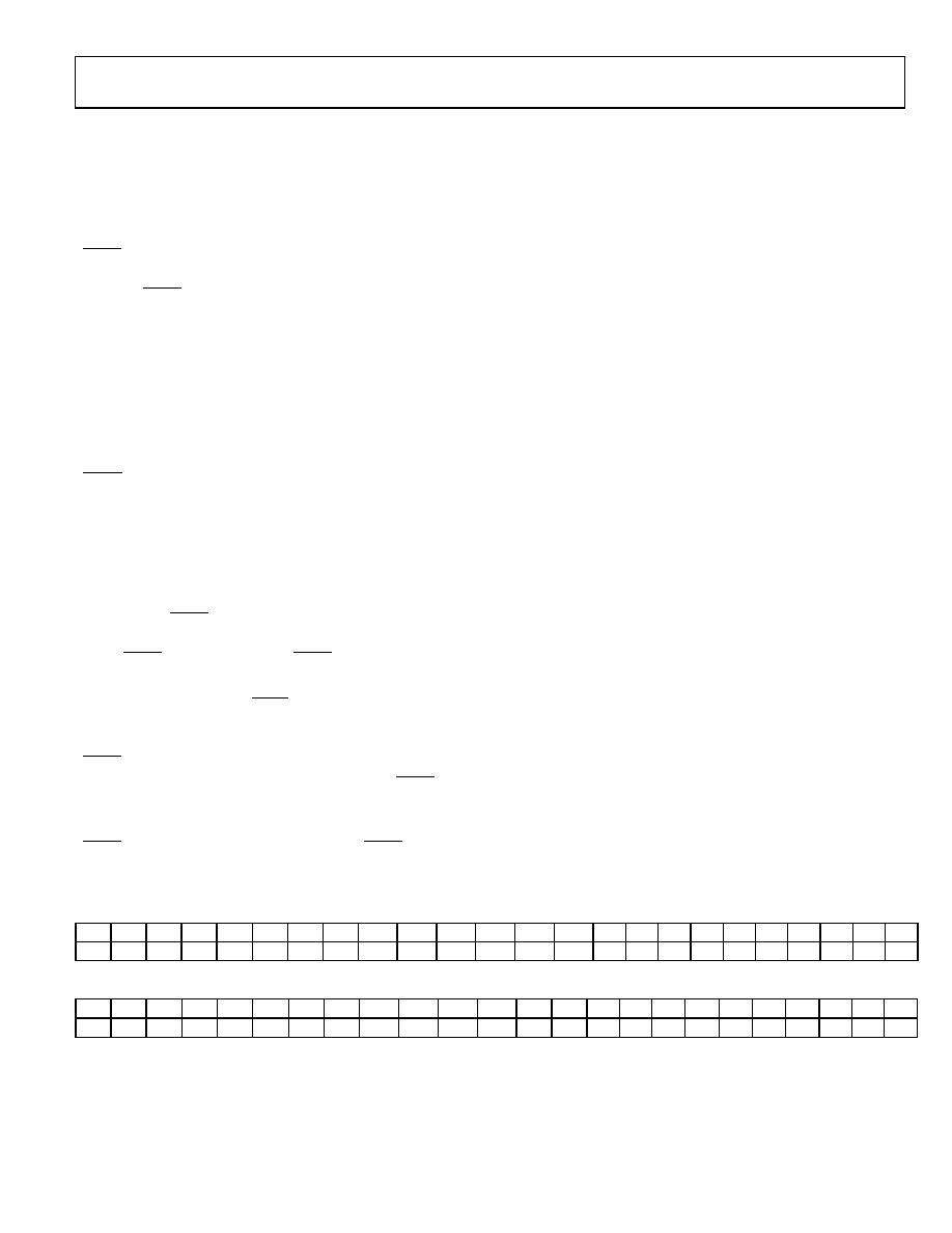
Table 11. AD5372 Serial Word Bit Assignment
I23
I22
I21
I20
I19
I18
I17
I16
I15
I14
I13
I12
I11
I10
I9
I8
I7
I6
I5
I4
I3
I2
I1
I0
M1
M0
A5
A4
A3
A2
A1
A0
D15
D14
D13
D12
D11
D10
D9
D8
D7
D6
D5
D4
D3
D2
D1
D0
Table 12. AD5373 Serial Word Bit Assignment
I23
I22
I21
I20
I19
I18
I17
I16
I15
I14
I13
I12
I11
I10
I9
I8
I7
I6
I5
I4
I3
I2
M1
M0
A5
A4
A3
A2
A1
A0
D13
D12
D11
D10
D9
D8
D7
D6
D5
D4
D3
D2
D1
D0
0
1 Bit I1 and Bit I0 are reserved for future use and should be 0 when writing the serial word. These bits read back as 0.
相关PDF资料 |
PDF描述 |
|---|---|
| LTC1595AIS8#PBF | IC D/A CONV 16BIT MULTPLYNG8SOIC |
| VE-2TJ-MY-F3 | CONVERTER MOD DC/DC 36V 50W |
| VI-B4Z-MU-F4 | CONVERTER MOD DC/DC 2V 80W |
| LTC2757BILX#PBF | IC DAC 18BIT PAR 48LQFP |
| MS3114E22-41SY | CONN RCPT 41POS JAM NUT W/SCKT |
相关代理商/技术参数 |
参数描述 |
|---|---|
| AD5372BSTZ-REEL | 功能描述:IC DAC 16BIT 32CH SER 64-LQFP RoHS:是 类别:集成电路 (IC) >> 数据采集 - 数模转换器 系列:- 产品培训模块:Lead (SnPb) Finish for COTS Obsolescence Mitigation Program 标准包装:1,000 系列:- 设置时间:1µs 位数:8 数据接口:串行 转换器数目:8 电压电源:双 ± 功率耗散(最大):941mW 工作温度:0°C ~ 70°C 安装类型:表面贴装 封装/外壳:24-SOIC(0.295",7.50mm 宽) 供应商设备封装:24-SOIC W 包装:带卷 (TR) 输出数目和类型:8 电压,单极 采样率(每秒):* |
| AD5373BCPZ | 功能描述:数模转换器- DAC 32-CH 14-bit Serial bipolar DAC I.C. RoHS:否 制造商:Texas Instruments 转换器数量:1 DAC 输出端数量:1 转换速率:2 MSPs 分辨率:16 bit 接口类型:QSPI, SPI, Serial (3-Wire, Microwire) 稳定时间:1 us 最大工作温度:+ 85 C 安装风格:SMD/SMT 封装 / 箱体:SOIC-14 封装:Tube |
| AD5373BCPZ-RL7 | 功能描述:14 Bit Digital to Analog Converter 32 56-LFCSP-VQ (8x8) 制造商:analog devices inc. 系列:- 包装:带卷(TR) 零件状态:上次购买时间 位数:14 数模转换器数:32 建立时间:30μs 输出类型:Voltage - Buffered 差分输出:无 数据接口:SPI,DSP 参考类型:外部 电压 - 电源,模拟:9 V ~ 16.5 V,-4.5 V ~ 16.5 V 电压 - 电源,数字:2.5 V ~ 5.5 V INL/DNL(LSB):±1(最大),±1(最大) 架构:电阻串 DAC 工作温度:-40°C ~ 85°C 封装/外壳:56-VFQFN 裸露焊盘,CSP 供应商器件封装:56-LFCSP-VQ(8x8) 标准包装:1 |
| AD5373BSTZ | 功能描述:IC DAC 14BIT 32CH SER 64-LQFP RoHS:是 类别:集成电路 (IC) >> 数据采集 - 数模转换器 系列:- 产品培训模块:Lead (SnPb) Finish for COTS Obsolescence Mitigation Program 标准包装:1,000 系列:- 设置时间:1µs 位数:8 数据接口:串行 转换器数目:8 电压电源:双 ± 功率耗散(最大):941mW 工作温度:0°C ~ 70°C 安装类型:表面贴装 封装/外壳:24-SOIC(0.295",7.50mm 宽) 供应商设备封装:24-SOIC W 包装:带卷 (TR) 输出数目和类型:8 电压,单极 采样率(每秒):* |
| AD5373BSTZ-REEL | 功能描述:IC DAC 14BIT 32CH SER 64-LQFP RoHS:是 类别:集成电路 (IC) >> 数据采集 - 数模转换器 系列:- 产品培训模块:Lead (SnPb) Finish for COTS Obsolescence Mitigation Program 标准包装:1,000 系列:- 设置时间:1µs 位数:8 数据接口:串行 转换器数目:8 电压电源:双 ± 功率耗散(最大):941mW 工作温度:0°C ~ 70°C 安装类型:表面贴装 封装/外壳:24-SOIC(0.295",7.50mm 宽) 供应商设备封装:24-SOIC W 包装:带卷 (TR) 输出数目和类型:8 电压,单极 采样率(每秒):* |
发布紧急采购,3分钟左右您将得到回复。