参数资料
| 型号: | AD5372BSTZ |
| 厂商: | Analog Devices Inc |
| 文件页数: | 9/29页 |
| 文件大小: | 0K |
| 描述: | IC DAC 16BIT 32CH SER 64-LQFP |
| 产品培训模块: | Data Converter Fundamentals DAC Architectures |
| 标准包装: | 1 |
| 设置时间: | 20µs |
| 位数: | 16 |
| 数据接口: | 串行 |
| 转换器数目: | 32 |
| 电压电源: | 双 ± |
| 功率耗散(最大): | 520mW |
| 工作温度: | -40°C ~ 85°C |
| 安装类型: | 表面贴装 |
| 封装/外壳: | 64-LQFP |
| 供应商设备封装: | 64-LQFP(10x10) |
| 包装: | 托盘 |
| 输出数目和类型: | 32 电压,单极;32 电压,双极 |
| 采样率(每秒): | * |
| 产品目录页面: | 782 (CN2011-ZH PDF) |
| 配用: | EVAL-AD5372EBZ-ND - BOARD EVAL FOR AD5372 |
第1页第2页第3页第4页第5页第6页第7页第8页当前第9页第10页第11页第12页第13页第14页第15页第16页第17页第18页第19页第20页第21页第22页第23页第24页第25页第26页第27页第28页第29页
AD5372/AD5373
Rev. C | Page 16 of 28
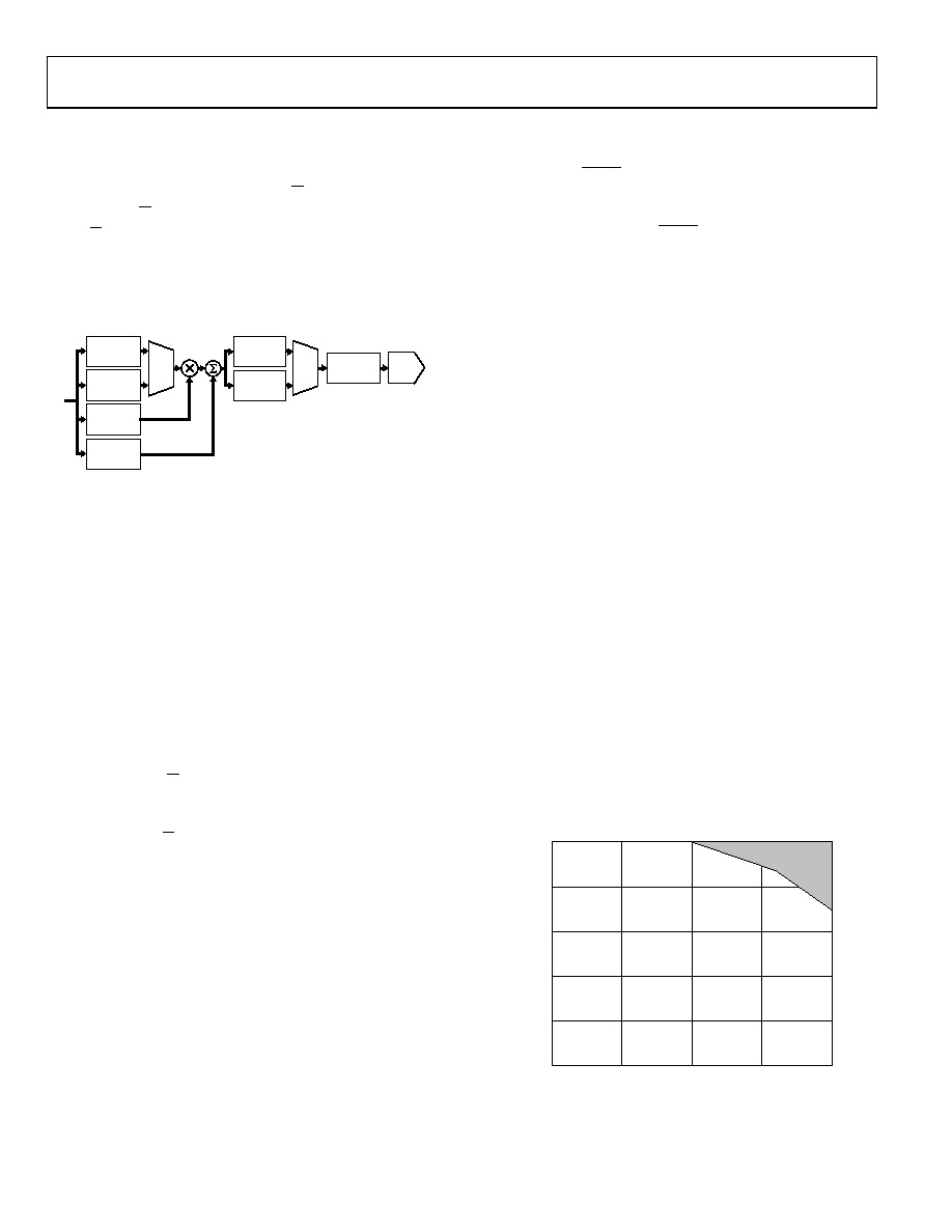
A/B REGISTERS AND GAIN/OFFSET ADJUSTMENT
Each DAC channel has seven data registers. The actual DAC
data-word can be written to either the X1A or the X1B input
register, depending on the setting of the A/B bit in the control
register. If the A/B bit is 0, data is written to the X1A register.
If the A/B bit is 1, data is written to the X1B register. Note that
this single bit is a global control and affects every DAC channel
in the device. It is not possible to set up the device on a per-
channel basis so that some writes are to X1A registers and
some writes are to X1B registers.
05
81
5-
0
18
MUX
DAC
REGISTER
MUX
X1A
REGISTER
X1B
REGISTER
M
REGISTER
C
REGISTER
X2A
REGISTER
X2B
REGISTER
Figure 19. Data Registers Associated with Each DAC Channel
Each DAC channel also has a gain (M) register and an offset
(C) register, which allow trimming out of the gain and offset
errors of the entire signal chain. Data from the X1A register is
operated on by a digital multiplier and adder controlled by the
contents of the M and C registers. The calibrated DAC data is
then stored in the X2A register. Similarly, data from the X1B
register is operated on by the multiplier and adder and stored in
the X2B register.
Although a multiplier and adder symbol are shown in Figure 19
for each channel, there is only one multiplier and one adder in the
device, which are shared among all channels. This has implica-
tions for the update speed when several channels are updated at
once, as described in the Register Update Rates section.
Each time data is written to the X1A register, or to the M or
C register with the A/B control bit set to 0, the X2A data is
recalculated and the X2A register is automatically updated.
Similarly, X2B is updated each time data is written to X1B,
or to M or C with A/B set to 1. The X2A and X2B registers
are not readable or directly writable by the user.
Data output from the X2A and X2B registers is routed to the
final DAC register by a multiplexer. Whether each individual
DAC takes its data from the X2A or from the X2B register is
controlled by an 8-bit A/B select register associated with each
group of eight DACs. If a bit in this register is 0, the DAC takes
its data from the X2A register; if 1, the DAC takes its data from
the X2B register (Bit 0 through Bit 7 control DAC 0 to DAC 7).
Note that because there are 32 bits in four registers, it is possible to
set up, on a per-channel basis, whether each DAC takes its data
from the X2A or X2B register. A global command is also provided
that sets all bits in the A/B select registers to 0 or to 1.
LOAD DAC
All DACs in the AD5372/AD5373 can be updated simultane-
ously by taking LDAC low when each DAC register is updated
from either its X2A or X2B register, depending on the setting
of the A/B select registers. The DAC register is not readable or
directly writable by the user. LDAC can be permanently tied
low, and the DAC output is updated whenever new data appears
in the appropriate DAC register.
OFFSET DACs
In addition to the gain and offset trim for each DAC, there are
two 14-bit offset DACs, one for Group 0 and one for Group 1 to
Group 3. These allow the output range of all DACs connected to
them to be offset within a defined range. Thus, subject to the
limitations of headroom, it is possible to set the output range of
Group 0 or Group 1 to Group 3 to be unipolar positive, unipolar
negative, or bipolar, either symmetrical or asymmetrical about
0 V. The DACs in the AD5372/AD5373 are factory trimmed with
the offset DACs set at their default values. This gives the best offset
and gain performance for the default output range and span.
When the output range is adjusted by changing the value of the
offset DAC, an extra offset is introduced due to the gain error of
the offset DAC. The amount of offset is dependent on the
magnitude of the reference and how much the offset DAC
moves from its default value. See the Specifications section for
this offset. The worst-case offset occurs when the offset DAC is
at positive or negative full scale. This value can be added to the
offset present in the main DAC channel to give an indication of
the overall offset for that channel. In most cases, the offset can
be removed by programming the C register of the channel with
an appropriate value. The extra offset caused by the offset DAC
needs to be taken into account only when the offset DAC is
changed from its default value. Figure 20 shows the allowable
code range that can be loaded to the offset DAC, depending on
the reference value used. Thus, for a 5 V reference, the offset
DAC should not be programmed with a value greater than 8192
(0x2000).
5
0
16383
0
581
5-
0
19
OFFSET DAC CODE
VR
E
F
(
V)
4
3
2
1
4096
8192
12288
RESERVED
Figure 20. Offset DAC Code Range
相关PDF资料 |
PDF描述 |
|---|---|
| LTC1595AIS8#PBF | IC D/A CONV 16BIT MULTPLYNG8SOIC |
| VE-2TJ-MY-F3 | CONVERTER MOD DC/DC 36V 50W |
| VI-B4Z-MU-F4 | CONVERTER MOD DC/DC 2V 80W |
| LTC2757BILX#PBF | IC DAC 18BIT PAR 48LQFP |
| MS3114E22-41SY | CONN RCPT 41POS JAM NUT W/SCKT |
相关代理商/技术参数 |
参数描述 |
|---|---|
| AD5372BSTZ-REEL | 功能描述:IC DAC 16BIT 32CH SER 64-LQFP RoHS:是 类别:集成电路 (IC) >> 数据采集 - 数模转换器 系列:- 产品培训模块:Lead (SnPb) Finish for COTS Obsolescence Mitigation Program 标准包装:1,000 系列:- 设置时间:1µs 位数:8 数据接口:串行 转换器数目:8 电压电源:双 ± 功率耗散(最大):941mW 工作温度:0°C ~ 70°C 安装类型:表面贴装 封装/外壳:24-SOIC(0.295",7.50mm 宽) 供应商设备封装:24-SOIC W 包装:带卷 (TR) 输出数目和类型:8 电压,单极 采样率(每秒):* |
| AD5373BCPZ | 功能描述:数模转换器- DAC 32-CH 14-bit Serial bipolar DAC I.C. RoHS:否 制造商:Texas Instruments 转换器数量:1 DAC 输出端数量:1 转换速率:2 MSPs 分辨率:16 bit 接口类型:QSPI, SPI, Serial (3-Wire, Microwire) 稳定时间:1 us 最大工作温度:+ 85 C 安装风格:SMD/SMT 封装 / 箱体:SOIC-14 封装:Tube |
| AD5373BCPZ-RL7 | 功能描述:14 Bit Digital to Analog Converter 32 56-LFCSP-VQ (8x8) 制造商:analog devices inc. 系列:- 包装:带卷(TR) 零件状态:上次购买时间 位数:14 数模转换器数:32 建立时间:30μs 输出类型:Voltage - Buffered 差分输出:无 数据接口:SPI,DSP 参考类型:外部 电压 - 电源,模拟:9 V ~ 16.5 V,-4.5 V ~ 16.5 V 电压 - 电源,数字:2.5 V ~ 5.5 V INL/DNL(LSB):±1(最大),±1(最大) 架构:电阻串 DAC 工作温度:-40°C ~ 85°C 封装/外壳:56-VFQFN 裸露焊盘,CSP 供应商器件封装:56-LFCSP-VQ(8x8) 标准包装:1 |
| AD5373BSTZ | 功能描述:IC DAC 14BIT 32CH SER 64-LQFP RoHS:是 类别:集成电路 (IC) >> 数据采集 - 数模转换器 系列:- 产品培训模块:Lead (SnPb) Finish for COTS Obsolescence Mitigation Program 标准包装:1,000 系列:- 设置时间:1µs 位数:8 数据接口:串行 转换器数目:8 电压电源:双 ± 功率耗散(最大):941mW 工作温度:0°C ~ 70°C 安装类型:表面贴装 封装/外壳:24-SOIC(0.295",7.50mm 宽) 供应商设备封装:24-SOIC W 包装:带卷 (TR) 输出数目和类型:8 电压,单极 采样率(每秒):* |
| AD5373BSTZ-REEL | 功能描述:IC DAC 14BIT 32CH SER 64-LQFP RoHS:是 类别:集成电路 (IC) >> 数据采集 - 数模转换器 系列:- 产品培训模块:Lead (SnPb) Finish for COTS Obsolescence Mitigation Program 标准包装:1,000 系列:- 设置时间:1µs 位数:8 数据接口:串行 转换器数目:8 电压电源:双 ± 功率耗散(最大):941mW 工作温度:0°C ~ 70°C 安装类型:表面贴装 封装/外壳:24-SOIC(0.295",7.50mm 宽) 供应商设备封装:24-SOIC W 包装:带卷 (TR) 输出数目和类型:8 电压,单极 采样率(每秒):* |
发布紧急采购,3分钟左右您将得到回复。