- 您现在的位置:买卖IC网 > PDF目录10791 > AD5384BBC-3 (Analog Devices Inc)IC DAC 14BIT 40CH 3V 100-CSPBGA PDF资料下载
参数资料
| 型号: | AD5384BBC-3 |
| 厂商: | Analog Devices Inc |
| 文件页数: | 20/32页 |
| 文件大小: | 0K |
| 描述: | IC DAC 14BIT 40CH 3V 100-CSPBGA |
| 产品培训模块: | Data Converter Fundamentals DAC Architectures |
| 产品变化通告: | AD5384 Models Discontinuation 15/May/2012 |
| 标准包装: | 1 |
| 设置时间: | 8µs |
| 位数: | 14 |
| 数据接口: | 串行 |
| 转换器数目: | 40 |
| 电压电源: | 单电源 |
| 功率耗散(最大): | 80mW |
| 工作温度: | -40°C ~ 85°C |
| 安装类型: | 表面贴装 |
| 封装/外壳: | 100-LFBGA,CSPBGA |
| 供应商设备封装: | 100-CSBGA(10x10) |
| 包装: | 托盘 |
| 输出数目和类型: | 40 电压,单极 |
| 采样率(每秒): | 125k |
第1页第2页第3页第4页第5页第6页第7页第8页第9页第10页第11页第12页第13页第14页第15页第16页第17页第18页第19页当前第20页第21页第22页第23页第24页第25页第26页第27页第28页第29页第30页第31页第32页
Data Sheet
AD5384
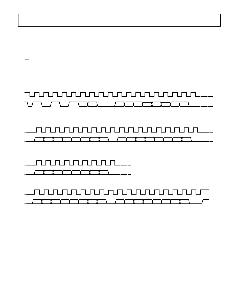
3-Byte Mode
In 3-byte mode, the user can update more than one channel in a
write sequence without having to write the device address byte
each time. The device address byte is required only once; sub-
sequent channel updates require the pointer byte and the data
bytes. In 3-byte mode, the use must begin with an address byte
(R/W = 0), after which the DAC acknowledges that it is prepared
to receive data by pulling SDA low. The address byte is followed
by the pointer byte. This addresses the specific channel in the
DAC to be addressed and also is acknowledged by the DAC.
This is then followed by the two data bytes, REG1 and REG0,
which determine the register to be updated.
If a stop condition does not follow the data bytes, another
channel can be updated by sending a new pointer byte, followed
by the data bytes. This mode requires only three bytes to be sent
to update any channel once the device is initially addressed, and
it reduces the software overhead in updating the AD5384 channels.
A stop condition at any time exits this mode. Figure 28 shows a
typical configuration.
SCL
SDA
SCL
SDA
SCL
SDA
SCL
START COND
BY MASTER
ACK BY
AD538x
MSB
ADDRESS BYTE
POINTER BYTE FOR CHANNEL N
MOST SIGNIFICANT DATA BYTE
POINTER BYTE FOR CHANNEL NEXT CHANNEL
LEAST SIGNIFICANT DATA BYTE
MOST SIGNIFICANT DATA BYTE
LEAST SIGNIFICANT DATA BYTE
ACK BY
AD538x
ACK BY
AD538x
DATA FOR CHANNEL N
DATA FOR CHANNEL NEXT CHANNEL
ACK BY
AD538x
1
0
A5
A4
A3
A2
A1
A0
0
1
0
A5
A4
A3
A2
A1
A0
1
AD1
AD0
R/W
REG1
REG0
MSB
LSB
MSB
LSB
MSB
ACK BY
AD538x
ACK BY
AD538x
ACK BY
AD538x
STOP COND
BY MASTER
REG1
REG0
MSB
LSB
MSB
LSB
04652-
030
Figure 28. 3-Byte, I2C Write Operation
Rev. B | Page 27 of 32
相关PDF资料 |
PDF描述 |
|---|---|
| AD5384BBC-3REEL7 | IC DAC 14BIT 40CH 3V 100-CSPBGA |
| ADCMP572BCPZ-R2 | IC COMPARATOR CML 3.3-5V 16LFCSP |
| LTC1687IS#PBF | IC TXRX RS485 PREC DELAY 14-SOIC |
| LTC1686IS8#PBF | IC TXRX RS485 PREC DELAY 8-SOIC |
| AD96687BQ | IC COMP DUAL 2.5NS 16-CDIP |
相关代理商/技术参数 |
参数描述 |
|---|---|
| AD5384BBC-3REEL7 | 功能描述:IC DAC 14BIT 40CH 3V 100-CSPBGA RoHS:否 类别:集成电路 (IC) >> 数据采集 - 数模转换器 系列:- 标准包装:2,400 系列:- 设置时间:- 位数:18 数据接口:串行 转换器数目:3 电压电源:模拟和数字 功率耗散(最大):- 工作温度:-40°C ~ 85°C 安装类型:表面贴装 封装/外壳:36-TFBGA 供应商设备封装:36-TFBGA 包装:带卷 (TR) 输出数目和类型:* 采样率(每秒):* |
| AD5384BBC-5 | 功能描述:IC DAC 14BIT 40CH 5V 100-CSPBGA RoHS:否 类别:集成电路 (IC) >> 数据采集 - 数模转换器 系列:- 标准包装:2,400 系列:- 设置时间:- 位数:18 数据接口:串行 转换器数目:3 电压电源:模拟和数字 功率耗散(最大):- 工作温度:-40°C ~ 85°C 安装类型:表面贴装 封装/外壳:36-TFBGA 供应商设备封装:36-TFBGA 包装:带卷 (TR) 输出数目和类型:* 采样率(每秒):* |
| AD5384BBC-5REEL7 | 功能描述:IC DAC 14BIT 40CH 5V 100-CSPBGA RoHS:否 类别:集成电路 (IC) >> 数据采集 - 数模转换器 系列:- 标准包装:2,400 系列:- 设置时间:- 位数:18 数据接口:串行 转换器数目:3 电压电源:模拟和数字 功率耗散(最大):- 工作温度:-40°C ~ 85°C 安装类型:表面贴装 封装/外壳:36-TFBGA 供应商设备封装:36-TFBGA 包装:带卷 (TR) 输出数目和类型:* 采样率(每秒):* |
| AD5384BBCZ-3 | 功能描述:IC DAC 14BIT 40CH 5V 100-CSPBGA RoHS:是 类别:集成电路 (IC) >> 数据采集 - 数模转换器 系列:- 标准包装:2,400 系列:- 设置时间:- 位数:18 数据接口:串行 转换器数目:3 电压电源:模拟和数字 功率耗散(最大):- 工作温度:-40°C ~ 85°C 安装类型:表面贴装 封装/外壳:36-TFBGA 供应商设备封装:36-TFBGA 包装:带卷 (TR) 输出数目和类型:* 采样率(每秒):* |
| AD5384BBCZ-5 | 功能描述:IC DAC 14BIT 40CH 5V 100-CSPBGA RoHS:是 类别:集成电路 (IC) >> 数据采集 - 数模转换器 系列:- 标准包装:2,400 系列:- 设置时间:- 位数:18 数据接口:串行 转换器数目:3 电压电源:模拟和数字 功率耗散(最大):- 工作温度:-40°C ~ 85°C 安装类型:表面贴装 封装/外壳:36-TFBGA 供应商设备封装:36-TFBGA 包装:带卷 (TR) 输出数目和类型:* 采样率(每秒):* |
发布紧急采购,3分钟左右您将得到回复。