- 您现在的位置:买卖IC网 > PDF目录10791 > AD5384BBC-3 (Analog Devices Inc)IC DAC 14BIT 40CH 3V 100-CSPBGA PDF资料下载
参数资料
| 型号: | AD5384BBC-3 |
| 厂商: | Analog Devices Inc |
| 文件页数: | 3/32页 |
| 文件大小: | 0K |
| 描述: | IC DAC 14BIT 40CH 3V 100-CSPBGA |
| 产品培训模块: | Data Converter Fundamentals DAC Architectures |
| 产品变化通告: | AD5384 Models Discontinuation 15/May/2012 |
| 标准包装: | 1 |
| 设置时间: | 8µs |
| 位数: | 14 |
| 数据接口: | 串行 |
| 转换器数目: | 40 |
| 电压电源: | 单电源 |
| 功率耗散(最大): | 80mW |
| 工作温度: | -40°C ~ 85°C |
| 安装类型: | 表面贴装 |
| 封装/外壳: | 100-LFBGA,CSPBGA |
| 供应商设备封装: | 100-CSBGA(10x10) |
| 包装: | 托盘 |
| 输出数目和类型: | 40 电压,单极 |
| 采样率(每秒): | 125k |
第1页第2页当前第3页第4页第5页第6页第7页第8页第9页第10页第11页第12页第13页第14页第15页第16页第17页第18页第19页第20页第21页第22页第23页第24页第25页第26页第27页第28页第29页第30页第31页第32页
Data Sheet
AD5384
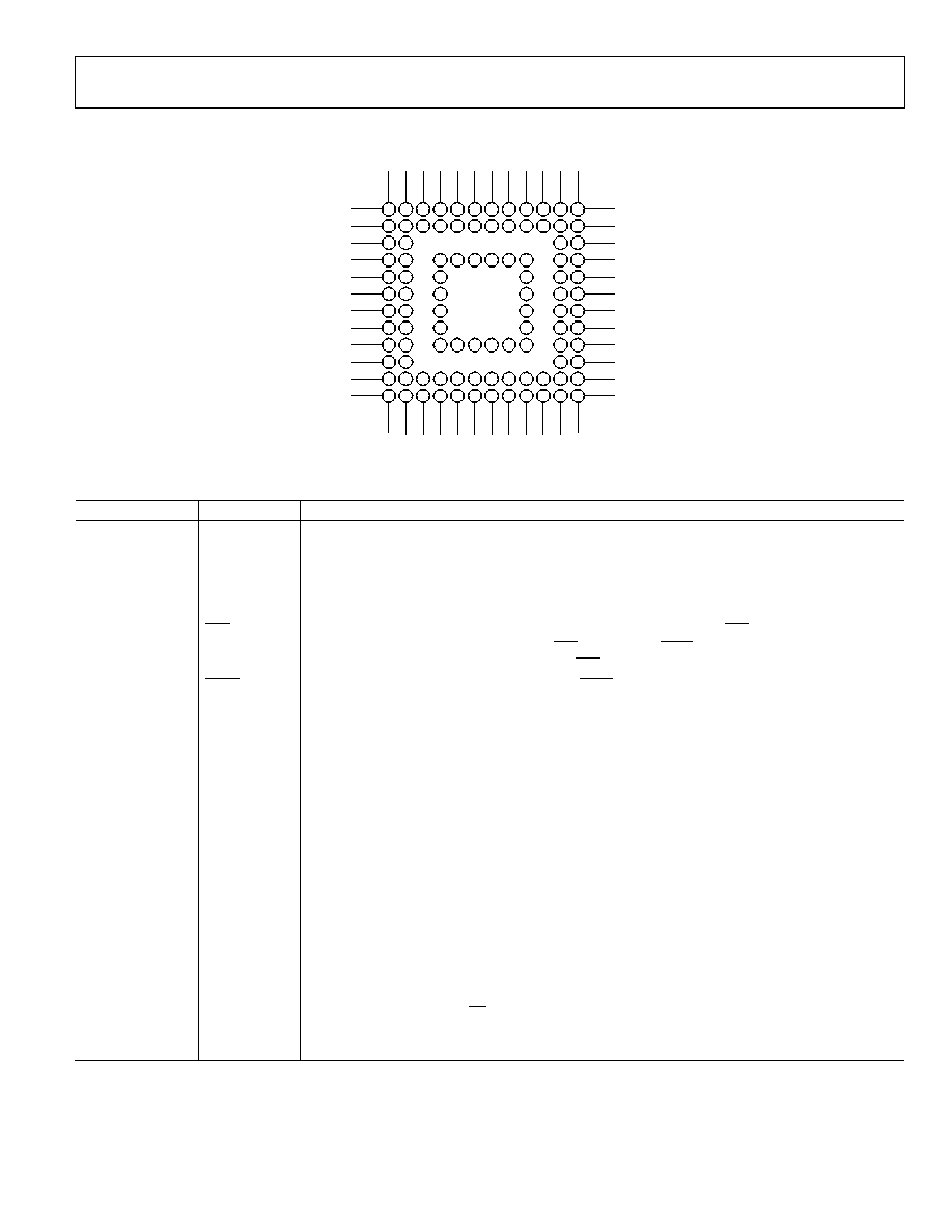
PIN CONFIGURATION AND FUNCTION DESCRIPTIONS
TOP VIEW
1
2
3
4
5
6
7
8
9
10 11 12
1
2
3
4
5
6
7
8
9
10 11 12
A
B
C
D
E
F
G
H
J
K
L
M
A
B
C
D
E
F
G
H
J
K
L
M
04652-
008
Figure 7. Pin Configuration
Table 6. Pin Function Descriptions
Pin No.
Mnemonic
Description
A1, A12, B2, B11,
C11, K11, L2, L11,
M1, M12
NC
No Connect. Do not connect to these pins.
A2
VOUT24
Buffered Analog Output. The analog output is driven by a rail-to-rail output amplifier operating at a
gain of 2. The output is capable of driving an output load of 5 k to ground.
Typical output impedance is 0.5 .
A3
CLR
Asynchronous Clear Input. The CLR input is falling edge sensitive. When CLR is activated, all
channels are updated with the data in the CLR code register. BUSY is low for a duration of 35 s
while all channels are being updated with the CLR code.
A4
SYNC/AD0
Multifunction Pin. In serial interface mode, the SYNC pin is the frame synchronization input signal
for the serial clocks before the address register is updated.
In I2C mode, AD0 acts as a hardware address pin used in conjunction with AD1 to determine the
software address for the device on the I2C bus.
A5
SCLK/SCL
Multifunction Pin. In serial interface mode, data is clocked into the shift register on the falling
edge of SCLK. SCLK operates at clock speeds up to 30 MHz.
In I2C mode, the SCL pin clocks data into the device. The data transfer rate in I2C mode is
compatible with both 100 kHz and 400 kHz operating modes.
A6, B6, D6
DVDD1 to
DVDD3
Logic Power Supply. Guaranteed operating range is 2.7 V to 5.5 V. Decouple these pins with
0.1 F ceramic and 10 F tantalum capacitors to DGND.
A7, B3, B7, D7
DGND
Ground for All Digital Circuitry.
A8
PD
Power-Down (Level Sensitive, Active High). Use PD to place the device in low power mode, where
AIDD reduces to 2 A and DIDD to 20 A. In power-down mode, all internal analog circuitry is placed
in low power mode, and the analog output is configured as a high impedance output or provides a
100 k load to ground, depending on how the power-down mode is configured. The serial interface
remains active during power-down.
A9
DCEN/AD1
Multifunction Pin. In SPI mode, the DCEN pin acts to enable the daisy-chain function. In I2C mode, the
AD1 pin acts as a hardware address pin.
Daisy-Chain Select Input (Level Sensitive, Active High). When DCEN is high, this pin is used
in conjunction with the SPI/I2C pin set high to enable the SPI serial interface in daisy-chain mode.
In I2C mode, the AD1 pin acts as a hardware address pin used in conjunction with AD0 to
determine the software address for this device on the I2C bus.
Rev. B | Page 11 of 32
相关PDF资料 |
PDF描述 |
|---|---|
| AD5384BBC-3REEL7 | IC DAC 14BIT 40CH 3V 100-CSPBGA |
| ADCMP572BCPZ-R2 | IC COMPARATOR CML 3.3-5V 16LFCSP |
| LTC1687IS#PBF | IC TXRX RS485 PREC DELAY 14-SOIC |
| LTC1686IS8#PBF | IC TXRX RS485 PREC DELAY 8-SOIC |
| AD96687BQ | IC COMP DUAL 2.5NS 16-CDIP |
相关代理商/技术参数 |
参数描述 |
|---|---|
| AD5384BBC-3REEL7 | 功能描述:IC DAC 14BIT 40CH 3V 100-CSPBGA RoHS:否 类别:集成电路 (IC) >> 数据采集 - 数模转换器 系列:- 标准包装:2,400 系列:- 设置时间:- 位数:18 数据接口:串行 转换器数目:3 电压电源:模拟和数字 功率耗散(最大):- 工作温度:-40°C ~ 85°C 安装类型:表面贴装 封装/外壳:36-TFBGA 供应商设备封装:36-TFBGA 包装:带卷 (TR) 输出数目和类型:* 采样率(每秒):* |
| AD5384BBC-5 | 功能描述:IC DAC 14BIT 40CH 5V 100-CSPBGA RoHS:否 类别:集成电路 (IC) >> 数据采集 - 数模转换器 系列:- 标准包装:2,400 系列:- 设置时间:- 位数:18 数据接口:串行 转换器数目:3 电压电源:模拟和数字 功率耗散(最大):- 工作温度:-40°C ~ 85°C 安装类型:表面贴装 封装/外壳:36-TFBGA 供应商设备封装:36-TFBGA 包装:带卷 (TR) 输出数目和类型:* 采样率(每秒):* |
| AD5384BBC-5REEL7 | 功能描述:IC DAC 14BIT 40CH 5V 100-CSPBGA RoHS:否 类别:集成电路 (IC) >> 数据采集 - 数模转换器 系列:- 标准包装:2,400 系列:- 设置时间:- 位数:18 数据接口:串行 转换器数目:3 电压电源:模拟和数字 功率耗散(最大):- 工作温度:-40°C ~ 85°C 安装类型:表面贴装 封装/外壳:36-TFBGA 供应商设备封装:36-TFBGA 包装:带卷 (TR) 输出数目和类型:* 采样率(每秒):* |
| AD5384BBCZ-3 | 功能描述:IC DAC 14BIT 40CH 5V 100-CSPBGA RoHS:是 类别:集成电路 (IC) >> 数据采集 - 数模转换器 系列:- 标准包装:2,400 系列:- 设置时间:- 位数:18 数据接口:串行 转换器数目:3 电压电源:模拟和数字 功率耗散(最大):- 工作温度:-40°C ~ 85°C 安装类型:表面贴装 封装/外壳:36-TFBGA 供应商设备封装:36-TFBGA 包装:带卷 (TR) 输出数目和类型:* 采样率(每秒):* |
| AD5384BBCZ-5 | 功能描述:IC DAC 14BIT 40CH 5V 100-CSPBGA RoHS:是 类别:集成电路 (IC) >> 数据采集 - 数模转换器 系列:- 标准包装:2,400 系列:- 设置时间:- 位数:18 数据接口:串行 转换器数目:3 电压电源:模拟和数字 功率耗散(最大):- 工作温度:-40°C ~ 85°C 安装类型:表面贴装 封装/外壳:36-TFBGA 供应商设备封装:36-TFBGA 包装:带卷 (TR) 输出数目和类型:* 采样率(每秒):* |
发布紧急采购,3分钟左右您将得到回复。