参数资料
| 型号: | AD5737ACPZ |
| 厂商: | Analog Devices Inc |
| 文件页数: | 21/44页 |
| 文件大小: | 0K |
| 描述: | IC DAC QUAD 12BIT CUR 64-LFCSP |
| 标准包装: | 1 |
| 设置时间: | 15µs |
| 位数: | 12 |
| 数据接口: | DSP,MICROWIRE?,QSPI?,串行,SPI? |
| 转换器数目: | 4 |
| 电压电源: | 模拟和数字 |
| 工作温度: | -40°C ~ 105°C |
| 安装类型: | 表面贴装 |
| 封装/外壳: | 64-VFQFN 裸露焊盘,CSP |
| 供应商设备封装: | 64-LFCSP-VQ(9x9) |
| 包装: | 托盘 |
| 输出数目和类型: | 4 电流,单极 |
| 采样率(每秒): | * |
第1页第2页第3页第4页第5页第6页第7页第8页第9页第10页第11页第12页第13页第14页第15页第16页第17页第18页第19页第20页当前第21页第22页第23页第24页第25页第26页第27页第28页第29页第30页第31页第32页第33页第34页第35页第36页第37页第38页第39页第40页第41页第42页第43页第44页
AD5737
Data Sheet
Rev. C | Page 28 of 44
CONTROL REGISTERS
When writing to a control register, the format shown in Table 18
must be used. See Table 11 for information about the configura-
tion of Bit D23 to Bit D16. The control registers are addressed
by setting the DREG[2:0] bits (Bits[D20:D18] in the input shift
register) to 111 and then setting the CREG[2:0] bits to select the
specific control register (see Table 19).
Main Control Register
The main control register options are shown in Table 20 and
Table 21. See the Device Features section for more information
about the features controlled by the main control register.
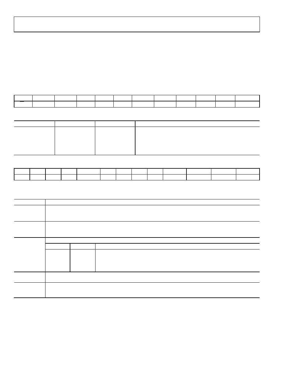
Table 18. Input Shift Register for a Write Operation to a Control Register
MSB
LSB
D23
D22
D21
D20
D19
D18
D17
D16
D15
D14
D13
D12 to D0
R/W
DUT_AD1
DUT_AD0
1
DAC_AD1
DAC_AD0
CREG2
CREG1
CREG0
Data
Table 19. Control Register Addresses (CREG[2:0] Bits)
CREG2 (D15)
CREG1 (D14)
CREG0 (D13)
Control Register
0
Slew rate control register (one per channel)
0
1
Main control register
0
1
0
DAC control register (one per channel)
0
1
DC-to-DC control register
1
0
Software register
Table 20. Programming the Main Control Register
D15
D14
D13
D12
D11
D10
D9
D8
D7
D6
D5
D4
D3 to D0
0
1
0
STATREAD
EWD
WD1
WD0
OUTEN_ALL DCDC_ALL
1 X = don’t care.
Table 21. Main Control Register Bit Descriptions
Bit Name
Description
STATREAD
Enable status readback during a write. See the Status Readback During a Write section.
0 = disable status readback (default).
1 = enable status readback.
EWD
Enable the watchdog timer. See the Watchdog Timer section.
0 = disable the watchdog timer (default).
1 = enable the watchdog timer.
WD1, WD0
Timeout select bits. Used to select the timeout period for the watchdog timer.
WD1
WD0
Timeout Period (ms)
0
5
0
1
10
1
0
100
1
200
OUTEN_ALL
Setting this bit to 1 enables the output on all four DACs simultaneously. Do not use the OUTEN_ALL bit when using the
OUTEN bit in the DAC control register.
DCDC_ALL
Setting this bit to 1 powers up the dc-to-dc converter on all four channels simultaneously. To power down the dc-to-dc
converters, all channel outputs must first be disabled. Do not use the DCDC_ALL bit when using the DC_DC bit in the
DAC control register.
相关PDF资料 |
PDF描述 |
|---|---|
| AD573JD | IC ADC 10BIT SAR REG 20-CDIP |
| AD5744RCSUZ-REEL7 | IC DAC QUAD 14BIT 1LSB 32TQFP |
| AD574AKPZ-REEL | IC ADC 12BIT W/REF/CLK 28-PLCC |
| AD5752AREZ | IC DAC DUAL 16BIT SERIAL 24TSSOP |
| AD5752RBREZ-REEL7 | IC DAC DUAL 16BIT SERIAL 24TSSOP |
相关代理商/技术参数 |
参数描述 |
|---|---|
| AD5737ACPZ-RL7 | 制造商:AD 制造商全称:Analog Devices 功能描述:Quad-Channel, 12-Bit, Serial Input, 4 mA to 20 mA Output |
| AD5737X | 制造商:AD 制造商全称:Analog Devices 功能描述:Quad Channel, 16-Bit, Serial Input, 4-20mA Output DAC, Dynamic Power Control, HART Connectivity |
| AD573JD | 功能描述:IC ADC 10BIT SAR REG 20-CDIP RoHS:否 类别:集成电路 (IC) >> 数据采集 - 模数转换器 系列:- 产品培训模块:Lead (SnPb) Finish for COTS Obsolescence Mitigation Program 标准包装:2,500 系列:- 位数:12 采样率(每秒):3M 数据接口:- 转换器数目:- 功率耗散(最大):- 电压电源:- 工作温度:- 安装类型:表面贴装 封装/外壳:SOT-23-6 供应商设备封装:SOT-23-6 包装:带卷 (TR) 输入数目和类型:- |
| AD573JN | 功能描述:IC ADC 10BIT SAR REGISTER 20-DIP RoHS:否 类别:集成电路 (IC) >> 数据采集 - 模数转换器 系列:- 标准包装:1 系列:- 位数:14 采样率(每秒):83k 数据接口:串行,并联 转换器数目:1 功率耗散(最大):95mW 电压电源:双 ± 工作温度:0°C ~ 70°C 安装类型:通孔 封装/外壳:28-DIP(0.600",15.24mm) 供应商设备封装:28-PDIP 包装:管件 输入数目和类型:1 个单端,双极 |
| AD573JNZ | 功能描述:IC ADC 10BIT SAR REGISTER 20-DIP RoHS:是 类别:集成电路 (IC) >> 数据采集 - 模数转换器 系列:- 标准包装:1 系列:microPOWER™ 位数:8 采样率(每秒):1M 数据接口:串行,SPI? 转换器数目:1 功率耗散(最大):- 电压电源:模拟和数字 工作温度:-40°C ~ 125°C 安装类型:表面贴装 封装/外壳:24-VFQFN 裸露焊盘 供应商设备封装:24-VQFN 裸露焊盘(4x4) 包装:Digi-Reel® 输入数目和类型:8 个单端,单极 产品目录页面:892 (CN2011-ZH PDF) 其它名称:296-25851-6 |
发布紧急采购,3分钟左右您将得到回复。