参数资料
| 型号: | AD5737ACPZ |
| 厂商: | Analog Devices Inc |
| 文件页数: | 27/44页 |
| 文件大小: | 0K |
| 描述: | IC DAC QUAD 12BIT CUR 64-LFCSP |
| 标准包装: | 1 |
| 设置时间: | 15µs |
| 位数: | 12 |
| 数据接口: | DSP,MICROWIRE?,QSPI?,串行,SPI? |
| 转换器数目: | 4 |
| 电压电源: | 模拟和数字 |
| 工作温度: | -40°C ~ 105°C |
| 安装类型: | 表面贴装 |
| 封装/外壳: | 64-VFQFN 裸露焊盘,CSP |
| 供应商设备封装: | 64-LFCSP-VQ(9x9) |
| 包装: | 托盘 |
| 输出数目和类型: | 4 电流,单极 |
| 采样率(每秒): | * |
第1页第2页第3页第4页第5页第6页第7页第8页第9页第10页第11页第12页第13页第14页第15页第16页第17页第18页第19页第20页第21页第22页第23页第24页第25页第26页当前第27页第28页第29页第30页第31页第32页第33页第34页第35页第36页第37页第38页第39页第40页第41页第42页第43页第44页
Data Sheet
AD5737
Rev. C | Page 33 of 44
DEVICE FEATURES
FAULT OUTPUT
The AD5737 is equipped with a FAULT pin, an active low,
open-drain output that allows several AD5737 devices to be
connected together to one pull-up resistor for global fault
detection. The FAULT pin is forced active by any one of the
following fault conditions:
The voltage at IOUT_x attempts to rise above the compliance
range due to an open-loop circuit or insufficient power
supply voltage. The internal circuitry that develops the
fault output avoids using a comparator with windowed
limits because this requires an actual output error before
the FAULT output becomes active. Instead, the signal is
generated when the internal amplifier in the output stage
has less than approximately 1 V of remaining drive
capability. Thus, the FAULT output is activated slightly
before the compliance limit is reached.
An interface error is detected due to a PEC failure (see the
Packet Error Checking section).
The core temperature of the AD5737 exceeds approxi-
mately 150°C.
The IOUT_x fault, PEC error, and over temp bits of the status
register are used in conjunction with the FAULT output to
inform the user which fault condition caused the FAULT
output to be activated.
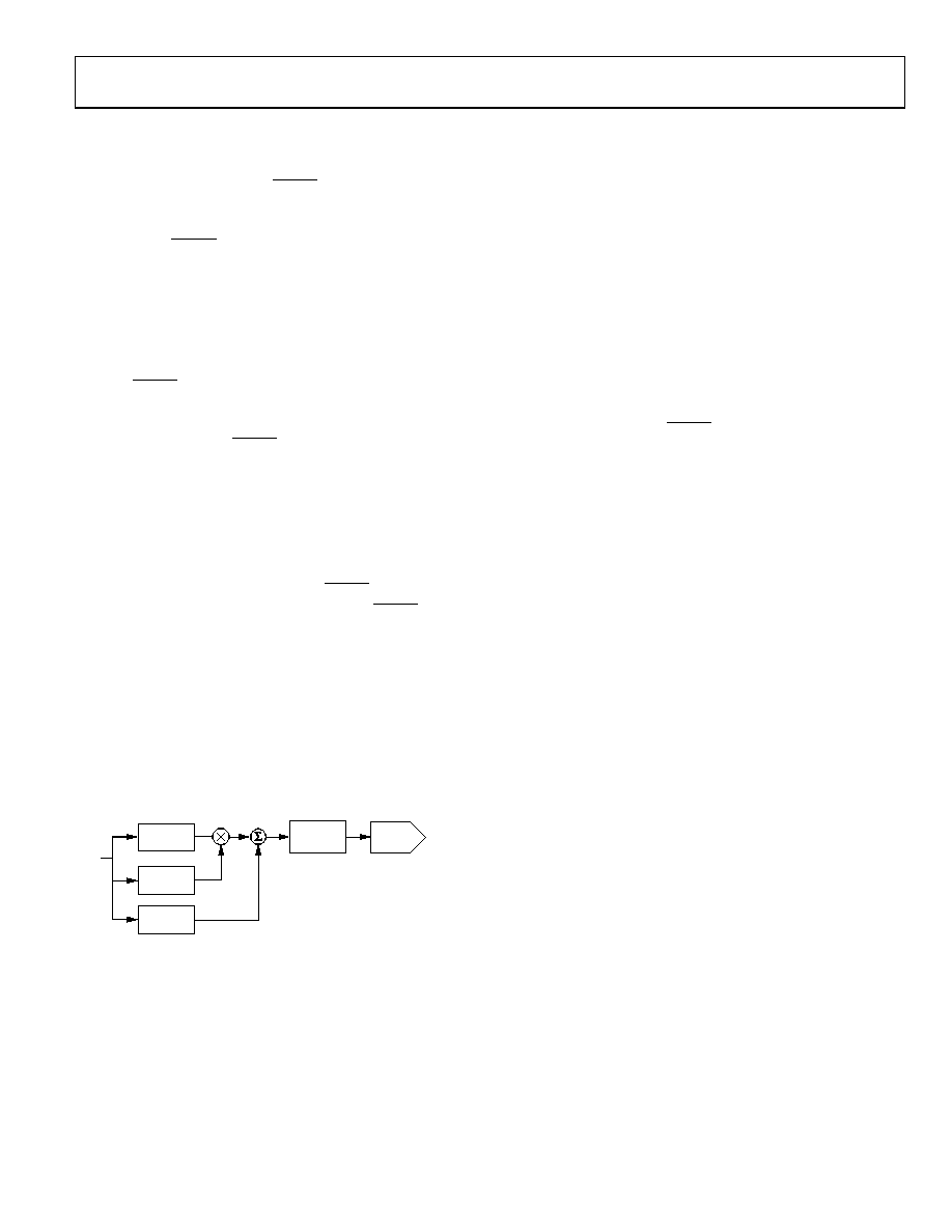
DIGITAL OFFSET AND GAIN CONTROL
Each DAC channel has a gain (M) register and an offset (C)
register, which allow trimming out of the gain and offset errors
of the entire signal chain. Data from the DAC data register is
operated on by a digital multiplier and adder controlled by the
contents of the gain and offset registers; the calibrated DAC
data is then stored in the DAC input register (see Figure 52).
DAC
INPUT
REGISTER
DAC
DAC DATA
REGISTER
GAIN (M)
REGISTER
OFFSET (C)
REGISTER
10067-
075
Figure 52. Digital Offset and Gain Control
Although Figure 52 indicates a multiplier and adder for each
channel, the device has only one multiplier and one adder,
which are shared by all four channels. This design has impli-
cations for the update speed when several channels are updated
at once (see Table 3).
When data is written to the gain (M) or offset (C) register, the
output is not automatically updated. Instead, the next write to
the DAC channel uses the new gain and offset values to perform
a new calibration and automatically updates the channel.
The output data from the calibration is routed to the DAC input
register. This data is then loaded to the DAC, as described in the
Serial Interface section. Both the gain register and the offset
register have 12 bits of resolution. The correct order to calibrate
the gain and offset is to first calibrate the gain and then calibrate
the offset.
The value (in decimal) that is written to the DAC input register
can be calculated as follows:
11
12
2
)
1
(
+
×
=
C
M
D
Code
r
DACRegiste
(1)
where:
D is the code loaded to the DAC data register of the
DAC channel.
M is the code in the gain register (default code = 212 1).
C is the code in the offset register (default code = 211).
STATUS READBACK DURING A WRITE
The AD5737 can be configured to read back the contents of
the status register during every write sequence. This feature is
enabled using the STATREAD bit in the main control register.
When this feature is enabled, the user can continuously monitor
the status register and act quickly in the case of a fault.
When status readback during a write is enabled, the contents
of the 16-bit status register (see Table 32) are output on the SDO
pin, as shown in Figure 5.
When the AD5737 is powered up, the status readback during a
write feature is disabled. When this feature is enabled, readback
of registers other than the status register is not available. To read
back any other register, clear the STATREAD bit before following
the readback sequence (see the Readback Operation section).
The STATREAD bit can be set high again after the register read.
ASYNCHRONOUS CLEAR
CLEAR is an active high, edge sensitive input that allows the
output to be cleared to a preprogrammed 12-bit code. This code
is user-programmable via a per-channel 12-bit clear code register.
For a channel to be cleared, set the CLR_EN bit in the DAC
control register for that channel. If the clear function on a
channel is not enabled, the output remains in its current state,
independent of the level of the CLEAR pin.
When the CLEAR signal returns low, the relevant outputs remain
cleared until a new value is programmed to them.
相关PDF资料 |
PDF描述 |
|---|---|
| AD573JD | IC ADC 10BIT SAR REG 20-CDIP |
| AD5744RCSUZ-REEL7 | IC DAC QUAD 14BIT 1LSB 32TQFP |
| AD574AKPZ-REEL | IC ADC 12BIT W/REF/CLK 28-PLCC |
| AD5752AREZ | IC DAC DUAL 16BIT SERIAL 24TSSOP |
| AD5752RBREZ-REEL7 | IC DAC DUAL 16BIT SERIAL 24TSSOP |
相关代理商/技术参数 |
参数描述 |
|---|---|
| AD5737ACPZ-RL7 | 制造商:AD 制造商全称:Analog Devices 功能描述:Quad-Channel, 12-Bit, Serial Input, 4 mA to 20 mA Output |
| AD5737X | 制造商:AD 制造商全称:Analog Devices 功能描述:Quad Channel, 16-Bit, Serial Input, 4-20mA Output DAC, Dynamic Power Control, HART Connectivity |
| AD573JD | 功能描述:IC ADC 10BIT SAR REG 20-CDIP RoHS:否 类别:集成电路 (IC) >> 数据采集 - 模数转换器 系列:- 产品培训模块:Lead (SnPb) Finish for COTS Obsolescence Mitigation Program 标准包装:2,500 系列:- 位数:12 采样率(每秒):3M 数据接口:- 转换器数目:- 功率耗散(最大):- 电压电源:- 工作温度:- 安装类型:表面贴装 封装/外壳:SOT-23-6 供应商设备封装:SOT-23-6 包装:带卷 (TR) 输入数目和类型:- |
| AD573JN | 功能描述:IC ADC 10BIT SAR REGISTER 20-DIP RoHS:否 类别:集成电路 (IC) >> 数据采集 - 模数转换器 系列:- 标准包装:1 系列:- 位数:14 采样率(每秒):83k 数据接口:串行,并联 转换器数目:1 功率耗散(最大):95mW 电压电源:双 ± 工作温度:0°C ~ 70°C 安装类型:通孔 封装/外壳:28-DIP(0.600",15.24mm) 供应商设备封装:28-PDIP 包装:管件 输入数目和类型:1 个单端,双极 |
| AD573JNZ | 功能描述:IC ADC 10BIT SAR REGISTER 20-DIP RoHS:是 类别:集成电路 (IC) >> 数据采集 - 模数转换器 系列:- 标准包装:1 系列:microPOWER™ 位数:8 采样率(每秒):1M 数据接口:串行,SPI? 转换器数目:1 功率耗散(最大):- 电压电源:模拟和数字 工作温度:-40°C ~ 125°C 安装类型:表面贴装 封装/外壳:24-VFQFN 裸露焊盘 供应商设备封装:24-VQFN 裸露焊盘(4x4) 包装:Digi-Reel® 输入数目和类型:8 个单端,单极 产品目录页面:892 (CN2011-ZH PDF) 其它名称:296-25851-6 |
发布紧急采购,3分钟左右您将得到回复。