参数资料
| 型号: | AD5737ACPZ |
| 厂商: | Analog Devices Inc |
| 文件页数: | 22/44页 |
| 文件大小: | 0K |
| 描述: | IC DAC QUAD 12BIT CUR 64-LFCSP |
| 标准包装: | 1 |
| 设置时间: | 15µs |
| 位数: | 12 |
| 数据接口: | DSP,MICROWIRE?,QSPI?,串行,SPI? |
| 转换器数目: | 4 |
| 电压电源: | 模拟和数字 |
| 工作温度: | -40°C ~ 105°C |
| 安装类型: | 表面贴装 |
| 封装/外壳: | 64-VFQFN 裸露焊盘,CSP |
| 供应商设备封装: | 64-LFCSP-VQ(9x9) |
| 包装: | 托盘 |
| 输出数目和类型: | 4 电流,单极 |
| 采样率(每秒): | * |
第1页第2页第3页第4页第5页第6页第7页第8页第9页第10页第11页第12页第13页第14页第15页第16页第17页第18页第19页第20页第21页当前第22页第23页第24页第25页第26页第27页第28页第29页第30页第31页第32页第33页第34页第35页第36页第37页第38页第39页第40页第41页第42页第43页第44页
Data Sheet
AD5737
Rev. C | Page 29 of 44
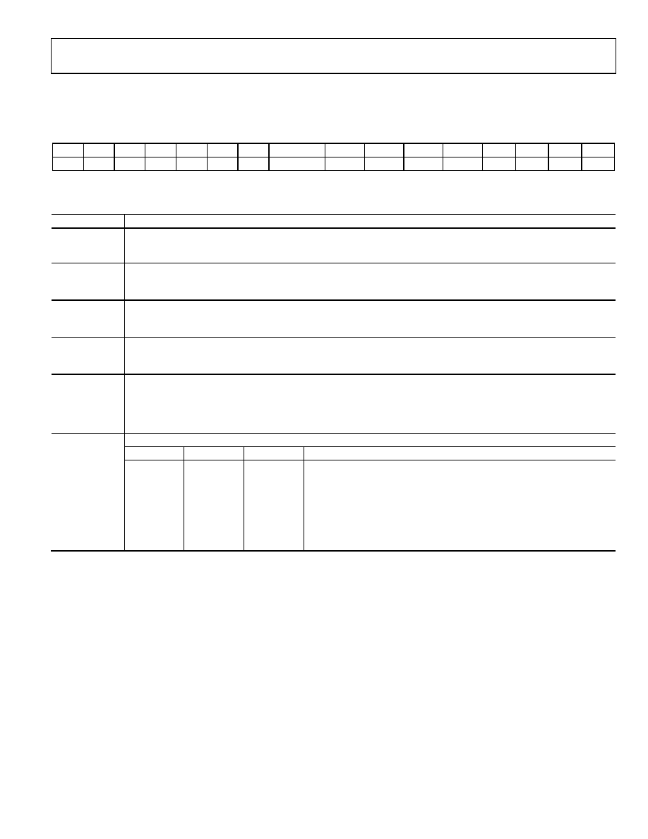
DAC Control Register
The DAC control register is used to configure each DAC channel. The DAC control register options are shown in Table 22 and Table 23.
Table 22. Programming the DAC Control Register
D15
D14
D13
D12
D11
D10
D9
D8
D7
D6
D5
D4
D3
D2
D1
D0
0
1
0
INT_ENABLE CLR_EN OUTEN RSET
DC_DC
R2
R1
R0
1 X = don’t care.
Table 23. DAC Control Register Bit Descriptions
Bit Name
Description
INT_ENABLE
Powers up the dc-to-dc converter, DAC, and internal amplifiers for the selected channel. This bit applies to individual
channels only; it does not enable the output. After setting this bit, it is recommended that a >200 s delay be observed
before enabling the output to reduce the output enable glitch. See Figure 24 for plots of this glitch.
CLR_EN
Per-channel clear enable bit. This bit specifies whether the selected channel is cleared when the CLEAR pin is activated.
0 = channel is not cleared when the part is cleared (default).
1 = channel is cleared when the part is cleared.
OUTEN
Enables or disables the selected output channel.
0 = channel disabled (default).
1 = channel enabled.
RSET
Selects the internal current sense resistor or an external current sense resistor for the selected DAC channel.
0 = external resistor selected (default).
1 = internal resistor selected.
DC_DC
Powers up or powers down the dc-to-dc converter on the selected channel. All dc-to-dc converters can be powered up
simultaneously using the DCDC_ALL bit in the main control register. To power down the dc-to-dc converter, the OUTEN
and INT_ENABLE bits must also be set to 0.
0 = dc-to-dc converter is powered down (default).
1 = dc-to-dc converter is powered up.
R2, R1, R0
Selects the output range to be enabled.
R2
R1
R0
Output Range Selected
0
Reserved
0
1
Reserved
0
1
0
Reserved
0
1
Reserved
1
0
4 mA to 20 mA current range
1
0
1
0 mA to 20 mA current range
1
0
0 mA to 24 mA current range
相关PDF资料 |
PDF描述 |
|---|---|
| AD573JD | IC ADC 10BIT SAR REG 20-CDIP |
| AD5744RCSUZ-REEL7 | IC DAC QUAD 14BIT 1LSB 32TQFP |
| AD574AKPZ-REEL | IC ADC 12BIT W/REF/CLK 28-PLCC |
| AD5752AREZ | IC DAC DUAL 16BIT SERIAL 24TSSOP |
| AD5752RBREZ-REEL7 | IC DAC DUAL 16BIT SERIAL 24TSSOP |
相关代理商/技术参数 |
参数描述 |
|---|---|
| AD5737ACPZ-RL7 | 制造商:AD 制造商全称:Analog Devices 功能描述:Quad-Channel, 12-Bit, Serial Input, 4 mA to 20 mA Output |
| AD5737X | 制造商:AD 制造商全称:Analog Devices 功能描述:Quad Channel, 16-Bit, Serial Input, 4-20mA Output DAC, Dynamic Power Control, HART Connectivity |
| AD573JD | 功能描述:IC ADC 10BIT SAR REG 20-CDIP RoHS:否 类别:集成电路 (IC) >> 数据采集 - 模数转换器 系列:- 产品培训模块:Lead (SnPb) Finish for COTS Obsolescence Mitigation Program 标准包装:2,500 系列:- 位数:12 采样率(每秒):3M 数据接口:- 转换器数目:- 功率耗散(最大):- 电压电源:- 工作温度:- 安装类型:表面贴装 封装/外壳:SOT-23-6 供应商设备封装:SOT-23-6 包装:带卷 (TR) 输入数目和类型:- |
| AD573JN | 功能描述:IC ADC 10BIT SAR REGISTER 20-DIP RoHS:否 类别:集成电路 (IC) >> 数据采集 - 模数转换器 系列:- 标准包装:1 系列:- 位数:14 采样率(每秒):83k 数据接口:串行,并联 转换器数目:1 功率耗散(最大):95mW 电压电源:双 ± 工作温度:0°C ~ 70°C 安装类型:通孔 封装/外壳:28-DIP(0.600",15.24mm) 供应商设备封装:28-PDIP 包装:管件 输入数目和类型:1 个单端,双极 |
| AD573JNZ | 功能描述:IC ADC 10BIT SAR REGISTER 20-DIP RoHS:是 类别:集成电路 (IC) >> 数据采集 - 模数转换器 系列:- 标准包装:1 系列:microPOWER™ 位数:8 采样率(每秒):1M 数据接口:串行,SPI? 转换器数目:1 功率耗散(最大):- 电压电源:模拟和数字 工作温度:-40°C ~ 125°C 安装类型:表面贴装 封装/外壳:24-VFQFN 裸露焊盘 供应商设备封装:24-VQFN 裸露焊盘(4x4) 包装:Digi-Reel® 输入数目和类型:8 个单端,单极 产品目录页面:892 (CN2011-ZH PDF) 其它名称:296-25851-6 |
发布紧急采购,3分钟左右您将得到回复。