- 您现在的位置:买卖IC网 > PDF目录8562 > AD5764CSUZ-REEL7 (Analog Devices Inc)IC DAC 16BIT QUAD BIPO 32-TQFP PDF资料下载
参数资料
| 型号: | AD5764CSUZ-REEL7 |
| 厂商: | Analog Devices Inc |
| 文件页数: | 14/28页 |
| 文件大小: | 0K |
| 描述: | IC DAC 16BIT QUAD BIPO 32-TQFP |
| 产品培训模块: | Data Converter Fundamentals DAC Architectures |
| 产品变化通告: | AD5764(R), AD5744R Product Change 04/Sept/2009 |
| 设计资源: | High Accuracy, Bipolar Voltage Output Digital-to-Analog Conversion Using AD5764 (CN0006) |
| 标准包装: | 500 |
| 设置时间: | 8µs |
| 位数: | 16 |
| 数据接口: | 串行 |
| 转换器数目: | 4 |
| 电压电源: | 双 ± |
| 功率耗散(最大): | 275 mW |
| 工作温度: | -40°C ~ 85°C |
| 安装类型: | 表面贴装 |
| 封装/外壳: | 32-TQFP |
| 供应商设备封装: | 32-TQFP(7x7) |
| 包装: | 带卷 (TR) |
| 输出数目和类型: | 4 电压,双极 |
| 采样率(每秒): | 1.26M |
| 配用: | EVAL-AD5764EBZ-ND - BOARD EVAL FOR AD5764 |
第1页第2页第3页第4页第5页第6页第7页第8页第9页第10页第11页第12页第13页当前第14页第15页第16页第17页第18页第19页第20页第21页第22页第23页第24页第25页第26页第27页第28页
Data Sheet
AD5764
Rev. F | Page 21 of 28
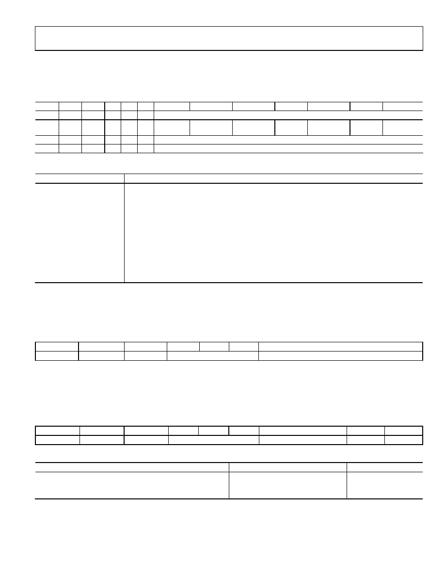
FUNCTION REGISTER
The function register is addressed by setting the three REG bits to 000. The values written to the address bits and the data bits determine
the function addressed. The functions available via the function register are outlined in Table 11 and Table 12.
Table 11. Function Register Options
REG2
REG1
REG0
A2
A1
A0
DB15:DB6
DB5
DB4
DB3
DB2
DB1
DB0
0
NOP, data = don’t care
0
1
Don’t care
Local ground
offset adjust
D1 direction
D1 value
D0 direction
D0 value
SDO disable
0
1
0
Clear, data = don’t care
0
1
0
1
Load, data = don’t care
Table 12. Explanation of Function Register Options
Option
Description
NOP
No operation instruction used in readback operations.
Local Ground Offset Adjust
Set by the user to enable the local ground offset adjust function. Cleared by the user to disable the local
ground offset adjust function (default). Refer to the Design Features section for further details.
D0/D1 Direction
Set by the user to enable D0/D1 as outputs. Cleared by the user to enable D0/D1 as inputs (default). Refer
to the Design Features section for further details.
D0/D1 Value
I/O port status bits. Logic values written to these locations determine the logic outputs on the D0 and D1
pins when configured as outputs. These bits indicate the status of the D0 and D1 pins when the I/O port is
active as an input. When enabled as inputs, these bits are don’t cares during a write operation.
SDO Disable
Set by the user to disable the SDO output. Cleared by the user to enable the SDO output (default).
Clear
Addressing this function resets the DAC outputs to 0 V in twos complement mode and negative full scale in
binary mode.
Load
Addressing this function updates the data register and consequently the analog outputs.
DATA REGISTER
The data register is addressed by setting the three REG bits to 010. The DAC address bits select with which DAC channel the data transfer
is to take place (see Table 10). The data bits are in Position DB15 to Position DB0, as shown in Table 13.
Table 13. Programming the Data Register Bit Map
REG2
REG1
REG0
A2
A1
A0
DB15:DB0
0
1
0
DAC address
16-bit DAC data
COARSE GAIN REGISTER
The coarse gain register is addressed by setting the three REG bits to 011. The DAC address bits select with which DAC channel the data
transfer is to take place (see Table 10). The coarse gain register is a 2-bit register and allows the user to select the output range of each
Table 14. Programming the Coarse Gain Register Bit Map
REG2
REG1
REG0
A2
A1
A0
DB15: DB2
DB1
DB0
0
1
DAC address
Don’t care
CG1
CG0
Table 15. Output Range Selection
Output Range
CG1
CG0
±10 V (Default)
0
±10.2564 V
0
1
±10.5263 V
1
0
相关PDF资料 |
PDF描述 |
|---|---|
| AD7834BRZ-REEL | IC DAC 14BIT QUAD SERIAL 28SOIC |
| MAX9654AUB+ | IC AMP FILTER W/SHUTDOWN 10-UMAX |
| DAC8420FS-REEL | IC DAC 12BIT QUAD SRL LP 16-SOIC |
| VI-BNV-MU-S | CONVERTER MOD DC/DC 5.8V 200W |
| LTC2704CGW-14#PBF | IC DAC 14BIT QUAD VOUT 44-SSOP |
相关代理商/技术参数 |
参数描述 |
|---|---|
| AD5764R | 制造商:AD 制造商全称:Analog Devices 功能描述:Complete Quad, 16-Bit, High Accuracy, Serial Input, Bipolar Voltage Output DAC |
| AD5764R_08 | 制造商:AD 制造商全称:Analog Devices 功能描述:Complete Quad, 16-Bit, High Accuracy, Serial Input, Bipolar Voltage Output DAC |
| AD5764RASUZ | 制造商:AD 制造商全称:Analog Devices 功能描述:Complete Quad, 16-Bit, High Accuracy, Serial Input, Bipolar Voltage Output DAC |
| AD5764RASUZ-REEL7 | 制造商:AD 制造商全称:Analog Devices 功能描述:Complete Quad, 16-Bit, High Accuracy, Serial Input, Bipolar Voltage Output DAC |
| AD5764RBSUZ | 功能描述:IC DAC 16BIT QUAD VOUT 32-TQFP RoHS:是 类别:集成电路 (IC) >> 数据采集 - 数模转换器 系列:- 产品培训模块:Lead (SnPb) Finish for COTS Obsolescence Mitigation Program 标准包装:1,000 系列:- 设置时间:1µs 位数:8 数据接口:串行 转换器数目:8 电压电源:双 ± 功率耗散(最大):941mW 工作温度:0°C ~ 70°C 安装类型:表面贴装 封装/外壳:24-SOIC(0.295",7.50mm 宽) 供应商设备封装:24-SOIC W 包装:带卷 (TR) 输出数目和类型:8 电压,单极 采样率(每秒):* |
发布紧急采购,3分钟左右您将得到回复。