- 您现在的位置:买卖IC网 > PDF目录1891 > AD5933YRSZ-REEL7 (Analog Devices Inc)NETWORK ANALYZER 12B 1MSP 16SSOP PDF资料下载
参数资料
| 型号: | AD5933YRSZ-REEL7 |
| 厂商: | Analog Devices Inc |
| 文件页数: | 24/40页 |
| 文件大小: | 0K |
| 描述: | NETWORK ANALYZER 12B 1MSP 16SSOP |
| 产品培训模块: | AD5933 Impedance to Digital Converter Direct Digital Synthesis Tutorial Series (1 of 7): Introduction Direct Digital Synthesizer Tutorial Series (7 of 7): DDS in Action Direct Digital Synthesis Tutorial Series (3 of 7): Angle to Amplitude Converter Direct Digital Synthesis Tutorial Series (6 of 7): SINC Envelope Correction Direct Digital Synthesis Tutorial Series (4 of 7): Digital-to-Analog Converter Direct Digital Synthesis Tutorial Series (2 of 7): The Accumulator |
| 标准包装: | 500 |
| 分辨率(位): | 12 b |
| 主 fclk: | 16.776MHz |
| 电源电压: | 2.7 V ~ 5.5 V |
| 工作温度: | -40°C ~ 125°C |
| 安装类型: | 表面贴装 |
| 封装/外壳: | 16-SSOP(0.209",5.30mm 宽) |
| 供应商设备封装: | 16-SSOP |
| 包装: | 带卷 (TR) |
| 配用: | EVAL-AD5933EBZ-ND - BOARD EVALUATION FOR AD5933 |
第1页第2页第3页第4页第5页第6页第7页第8页第9页第10页第11页第12页第13页第14页第15页第16页第17页第18页第19页第20页第21页第22页第23页当前第24页第25页第26页第27页第28页第29页第30页第31页第32页第33页第34页第35页第36页第37页第38页第39页第40页
AD5933
Data Sheet
Rev. E | Page 30 of 40
TYPICAL APPLICATIONS
MEASURING SMALL IMPEDANCES
The AD5933 is capable of measuring impedance values up to
10 MΩ if the system gain settings are chosen correctly for the
impedance subrange of interest.
If the user places a small impedance value (≤500 Ω over the
sweep frequency of interest) between the VOUT and VIN pins,
it results in an increase in signal current flowing through the
impedance for a fixed excitation voltage in accordance with
Ohm’s law. The output stage of the transmit side amplifier
available at the VOUT pin may not be able to provide the
required increase in current through the impedance. To have a
unity gain condition about the receive side I-V amplifier, the
user needs to have a similar small value of feedback resistance
for system calibration as outlined in the Gain Factor Setup
Configuration section. The voltage presented at the VIN pin is
hard biased at VDD/2 due to the virtual earth on the receive
side I-V amplifier. The increased current sink/source
requirement placed on the output of the receive side I-V
amplifier may also cause the amplifier to operate outside of
the linear region. This causes significant errors in subsequent
impedance measurements.
at the VOUT pin must be taken into account when measuring
small impedances (ZUNKNOWN), specifically when the value of
the output series resistance is comparable to the value of the
impedance under test (ZUNKNOWN). If the ROUT value is unac-
counted for in the system calibration (that is, the gain factor
calculation) when measuring small impedances, there is an
introduced error into any subsequent impedance measurement
that takes place. The introduced error depends on the relative
magnitude of the impedance being tested compared to the value
of the output series resistance.
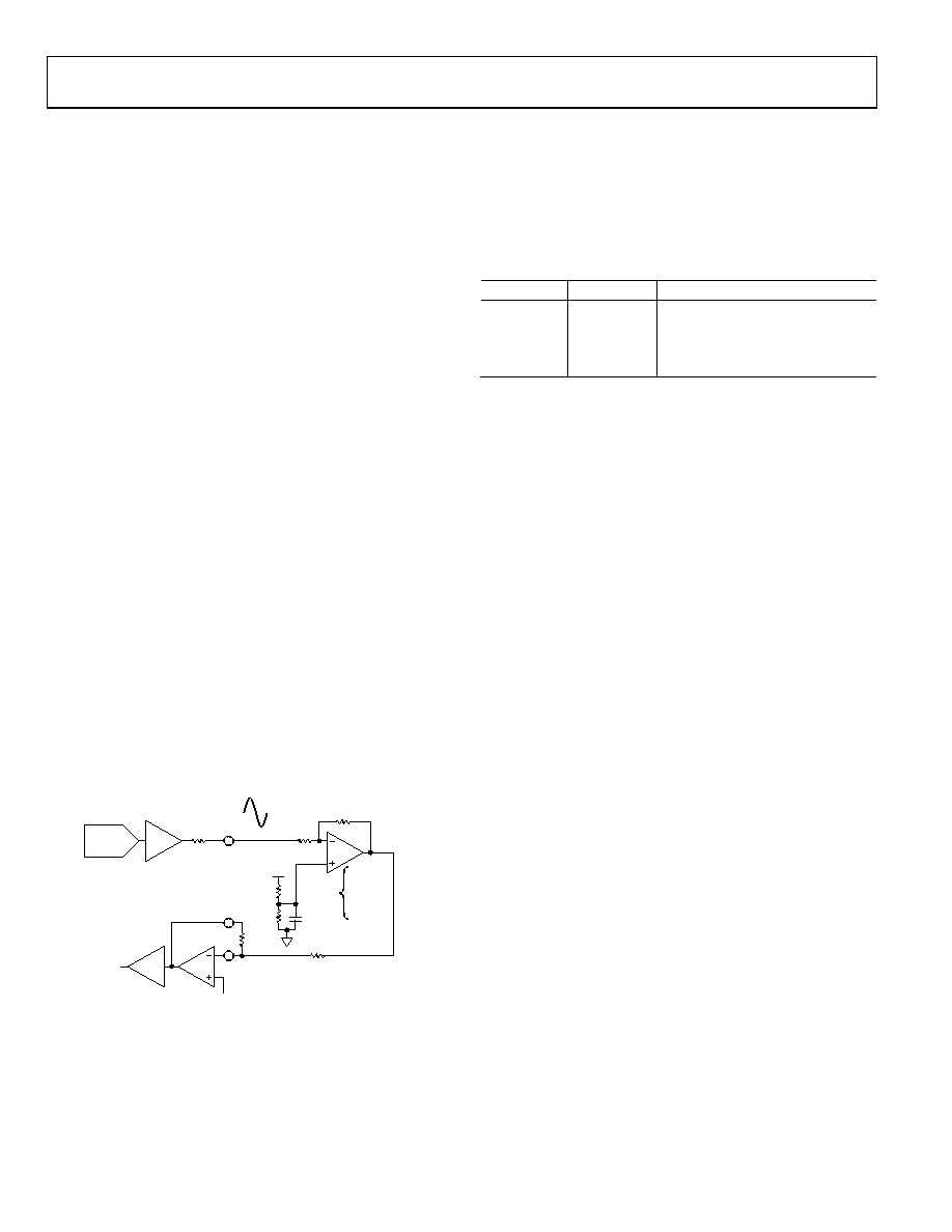
05324-
048
PGA
I-V
VDD/2
RFB
VIN
AD8531
AD820
AD8641
AD8627
VDD
20k
1F
VDD/2
VOUT
ROUT
RFB
DDS
2V p-p
R1
R2
ZUNKNOWN
TRANSMIT SIDE
OUTPUT AMPLIFIER
Figure 35. Additional External Amplifier Circuit for Measuring Small
Impedances
The value of the output series resistance depends upon the
selected output excitation range at VOUT and has a tolerance
from device to device like all discrete resistors manufactured in
a silicon fabrication process. Typical values of the output series
resistance are outlined in Table 17.
Table 17. Output Series Resistance (ROUT) vs. Excitation Range
Parameter
Value (Typ)
Output Series Resistance Value
Range 1
2 V p-p
200 typ
Range 2
1 V p-p
2.4 k typ
Range 3
0.4 V p-p
1.0 k typ
Range 4
0.2 V p-p
600 typ
Therefore, to accurately calibrate the AD5933 to measure small
impedances, it is necessary to reduce the signal current by
attenuating the excitation voltage sufficiently and also account
for the ROUT value and factor it into the gain factor calculation
(see the Gain Factor Calculation section).
Measuring the ROUT value during device characterization is
achieved by selecting the appropriate output excitation range at
VOUT and sinking and sourcing a known current at the pin
(for example, ±2 mA) and measuring the change in dc voltage.
The output series resistance can be calculated by measuring the
inverse of the slope (that is, 1/slope) of the resultant I-V plot.
A circuit that helps to minimize the effects of the issues
previously outlined is shown in Figure 35. The aim of this
circuit is to place the AD5933 system gain within its linear
range when measuring small impedances by using an additional
external amplifier circuit along the signal path. The external
amplifier attenuates the peak-to-peak excitation voltage at
VOUT by a suitable choice of resistors (R1 and R2), thereby
reducing the signal current flowing through the impedance and
minimizing the effect of the output series resistance in the
impedance calculations.
output series resistance of the external amplifier which is
typically much less than 1 Ω with feedback applied depending
AD8531) as well as the load current, bandwidth, and gain.
相关PDF资料 |
PDF描述 |
|---|---|
| AD5934YRSZ | IC NTWK ANALYZER 12B 1MSP 16SSOP |
| AD598JR | IC LVDT SGNL COND OSC/REF 20SOIC |
| AD660BR | IC DAC 16BIT MONO W/VREF 24-SOIC |
| AD6620ASZ | IC DGTL RCVR DUAL 67MSPS 80-PQFP |
| AD6623ASZ | IC TSP 4CHAN 104MSPS 128MQFP |
相关代理商/技术参数 |
参数描述 |
|---|---|
| AD5934 | 制造商:Analog Devices 功能描述:IMPEDANCE TO DIGITAL CONVERTERS - Bulk |
| AD5934YRSZ | 功能描述:IC NTWK ANALYZER 12B 1MSP 16SSOP RoHS:是 类别:集成电路 (IC) >> 接口 - 直接数字合成 (DDS) 系列:- 产品变化通告:Product Discontinuance 27/Oct/2011 标准包装:2,500 系列:- 分辨率(位):10 b 主 fclk:25MHz 调节字宽(位):32 b 电源电压:2.97 V ~ 5.5 V 工作温度:-40°C ~ 85°C 安装类型:表面贴装 封装/外壳:16-TSSOP(0.173",4.40mm 宽) 供应商设备封装:16-TSSOP 包装:带卷 (TR) |
| AD5934YRSZ-REEL7 | 功能描述:IC CONV 12BIT 250KSPS 16SSOP RoHS:是 类别:集成电路 (IC) >> 接口 - 直接数字合成 (DDS) 系列:- 产品变化通告:Product Discontinuance 27/Oct/2011 标准包装:2,500 系列:- 分辨率(位):10 b 主 fclk:25MHz 调节字宽(位):32 b 电源电压:2.97 V ~ 5.5 V 工作温度:-40°C ~ 85°C 安装类型:表面贴装 封装/外壳:16-TSSOP(0.173",4.40mm 宽) 供应商设备封装:16-TSSOP 包装:带卷 (TR) |
| AD594 | 制造商:AD 制造商全称:Analog Devices 功能描述:Monolithic Thermocouple Amplifiers with Cold Junction Compensation |
| AD594A | 制造商:AD 制造商全称:Analog Devices 功能描述:Monolithic Thermocouple Amplifiers with Cold Junction Compensation |
发布紧急采购,3分钟左右您将得到回复。