- 您现在的位置:买卖IC网 > PDF目录373890 > AD6620AS (ANALOG DEVICES INC) 65 MSPS Digital Receive Signal Processor PDF资料下载
参数资料
| 型号: | AD6620AS |
| 厂商: | ANALOG DEVICES INC |
| 元件分类: | 微控制器/微处理器 |
| 英文描述: | 65 MSPS Digital Receive Signal Processor |
| 中文描述: | SPECIALTY MICROPROCESSOR CIRCUIT, PQFP80 |
| 封装: | PLASTIC, QFP-80 |
| 文件页数: | 17/43页 |
| 文件大小: | 354K |
| 代理商: | AD6620AS |
第1页第2页第3页第4页第5页第6页第7页第8页第9页第10页第11页第12页第13页第14页第15页第16页当前第17页第18页第19页第20页第21页第22页第23页第24页第25页第26页第27页第28页第29页第30页第31页第32页第33页第34页第35页第36页第37页第38页第39页第40页第41页第42页第43页
AD6620
–17–
REV. 0
Diversity Channel Real Mode
In the Diversity Channel Real mode the A/B pin serves not only
as an input enable but also to determine which channel is being
sampled on a given CLK edge. A high on the A/B pin marks
channel A data and a low on A/B marks channel B data. The
AD6620 only accepts the first sample after an A/B transition.
All subsequent samples are disregarded until A/B changes again.
When full rate input timing is employed in the Diversity Chan-
nel Real mode, A/B must toggle on every edge of CLK for new
data to be clocked into the AD6620.
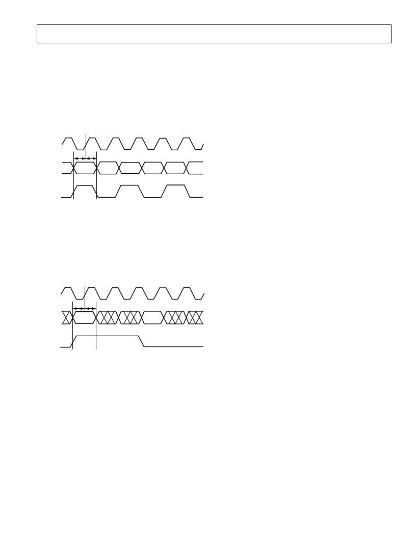
t
SI
t
HI
CLK
IN[15:0]
EXP[2:0]
A/B
A
N
B
N
B
N+1
A
N+1
A
N+2
B
N+2
Figure 30. Full Rate Input Timing, Diversity Channel Real
Mode
If fractional rate input timing is necessary in the Diversity Chan-
nel Real Mode, the A/B pin must toggle at half the rate of the
A/D sample clock. The timing diagram below shows a 3
×
pro-
cessing clock. In this situation there will be one ADC encode
pulse for every three AD6620 CLK pulses and data must be
taken on every third CLK pulse. The CLK edges that corre-
spond to the latching of A and B channel data are shown in
Figure 31.
A
N
t
SI
t
HI
CLK
IN[15:0]
EXP[2:0]
A/B
B
N
Figure 31. Fractional Rate Input Timing (3
×
CLK), Diversity
Channel Real Mode
Single Channel Complex Mode
In the Single Channel Complex input mode, A/B high identi-
fies the in-phase samples and A/B low identifies quadrature
samples. The quadrature samples are paired with the previous
in-phase samples. The timing for this mode is the same as that
of the Diversity Channel Real Mode. This mode is useful for
accepting complex output data from another AD6620 or an-
other source to increase filtering and or decimation rates.
In the Single Channel Complex Mode the CIC2 decimation
must be set to two (M
CIC2
= 2). This is necessary in order to
allow enough CLK cycles to process the complex input data as
described below.
First clock cycle: (A/B high).
– I data loaded from the input port.
– The I data-path gets I
×
cosine.
– The Q data-path gets I
×
sine.
– The first integrator of the CIC2 adds these values to its
previous sums.
– The rest of the CIC2 is idle.
Second clock cycle: (A/B low).
– Q data loaded from the input port.
– The I data-path gets Q
×
sine.
– The Q data-path gets Q
×
cosine.
– The first integrator of the I path of the CIC2 completes the
sum (I
×
cosine - Q
×
sine) and the first integrator of the Q
path of the CIC2 completes the sum j(I
×
sine + Q
×
cosine).
– The rest of the CIC2 operates on these sums, which is the
complete complex multiply. The data is then multiplexed
through the rest of the chip as if it were single channel real data.
相关PDF资料 |
PDF描述 |
|---|---|
| AD6620S | 65 MSPS Digital Receive Signal Processor |
| AD6620 | 65 MSPS Digital Receive Signal Processor(采样速率65MSPS的数字接收信号处理器) |
| AD6622AS | Four-Channel, 75 MSPS Digital Transmit Signal Processor TSP |
| AD6622PCB | Four-Channel, 75 MSPS Digital Transmit Signal Processor TSP |
| AD6622S | Four-Channel, 75 MSPS Digital Transmit Signal Processor TSP |
相关代理商/技术参数 |
参数描述 |
|---|---|
| AD6620AS-REEL | 制造商:Analog Devices 功能描述:Signal Processor 80-Pin PQFP T/R |
| AD6620ASZ | 功能描述:IC DGTL RCVR DUAL 67MSPS 80-PQFP RoHS:是 类别:集成电路 (IC) >> 接口 - 专用 系列:- 特色产品:NXP - I2C Interface 标准包装:1 系列:- 应用:2 通道 I²C 多路复用器 接口:I²C,SM 总线 电源电压:2.3 V ~ 5.5 V 封装/外壳:16-TSSOP(0.173",4.40mm 宽) 供应商设备封装:16-TSSOP 包装:剪切带 (CT) 安装类型:表面贴装 产品目录页面:825 (CN2011-ZH PDF) 其它名称:568-1854-1 |
| AD6620ASZ-REEL | 功能描述:IC DGTL RCVR DUAL 67MSPS 80-PQFP RoHS:是 类别:集成电路 (IC) >> 接口 - 专用 系列:- 特色产品:NXP - I2C Interface 标准包装:1 系列:- 应用:2 通道 I²C 多路复用器 接口:I²C,SM 总线 电源电压:2.3 V ~ 5.5 V 封装/外壳:16-TSSOP(0.173",4.40mm 宽) 供应商设备封装:16-TSSOP 包装:剪切带 (CT) 安装类型:表面贴装 产品目录页面:825 (CN2011-ZH PDF) 其它名称:568-1854-1 |
| AD6620PCB | 制造商:AD 制造商全称:Analog Devices 功能描述:65 MSPS Digital Receive Signal Processor |
| AD6620S | 制造商:AD 制造商全称:Analog Devices 功能描述:65 MSPS Digital Receive Signal Processor |
发布紧急采购,3分钟左右您将得到回复。