- 您现在的位置:买卖IC网 > PDF目录10097 > AD7703AR (Analog Devices Inc)IC ADC 20BIT LC2MOS 20-SOIC PDF资料下载
参数资料
| 型号: | AD7703AR |
| 厂商: | Analog Devices Inc |
| 文件页数: | 2/16页 |
| 文件大小: | 0K |
| 描述: | IC ADC 20BIT LC2MOS 20-SOIC |
| 标准包装: | 1 |
| 位数: | 20 |
| 采样率(每秒): | 4k |
| 数据接口: | 串行 |
| 转换器数目: | 1 |
| 功率耗散(最大): | 37mW |
| 电压电源: | 模拟和数字,双 ± |
| 工作温度: | -40°C ~ 85°C |
| 安装类型: | 表面贴装 |
| 封装/外壳: | 20-SOIC(0.295",7.50mm 宽) |
| 供应商设备封装: | 20-SOIC W |
| 包装: | 管件 |
| 输入数目和类型: | 1 个单端,单极;1 个单端,双极 |
REV. E
–10–
AD7703
Initiating Calibration
Table III illustrates the calibration modes available in the AD7703.
Not shown in the table is the function of the BP/
UP pin, which
determines whether the converter has been calibrated to mea-
sure bipolar or unipolar signals. A calibration step is initiated by
bringing the CAL pin high for at least four CLKIN cycles and
then bringing it low again. The states of SC1 and SC2 along
with the BP/
UP pin will determine the type of calibration to be
performed. All three signals should be stable before the CAL
pin is taken positive. The SC1 and SC2 inputs are latched when
CAL goes high. The BP/
UP input is not latched and, therefore,
must remain in a fixed state throughout the calibration and
measurement cycles. Any time the state of the BP/
UP is changed,
a new calibration cycle must be performed to enable the AD7703
to function properly in the new mode.
When a calibration step is initiated, the
DRDY signal will go high
and remain high until the step is finished. Table III shows the
number of clock cycles each calibration requires. Once a calibra-
tion step is initiated, it must finish before a new calibration step
can be executed. In the two step system calibration mode, the
offset calibration step must be initiated before initiating the gain
calibration step.
When self-calibration is completed,
DRDY falls and the output
port is updated with a data-word that represents the analog input
signal. When a system calibration step is completed,
DRDY will
fall and the output port will be updated with the appropriate data
value (all 0s for the zero-scale point and all 1s for the full-scale
point). In the system calibration mode, the digital filter must
settle before the output code will represent the value of the
analog input signal. Tables IV and V indicate the output code
size and output coding of the AD7703 in its various modes. In
these tables, SOFF is the measured system offset in volts and
SGAIN is the measured system gain at the full-scale point in volts.
Span and Offset Limits
Whenever a system calibration mode is used, there are limits
on the amount of offset and span that can be accommodated.
The range of input span in both the Unipolar and Bipolar
modes has a minimum value of 0.8 VREF and a maximum
value of 2(VREF + 0.1 V).
The amount of offset that can be accommodated depends on
whether the Unipolar or Bipolar mode is being used. In Unipolar
mode, the system calibration modes can handle a maximum
offset of 0.2 VREF and a minimum offset of –(VREF + 0.1 V).
Therefore the AD7703 in the Unipolar mode can be calibrated
to mimic bipolar operation.
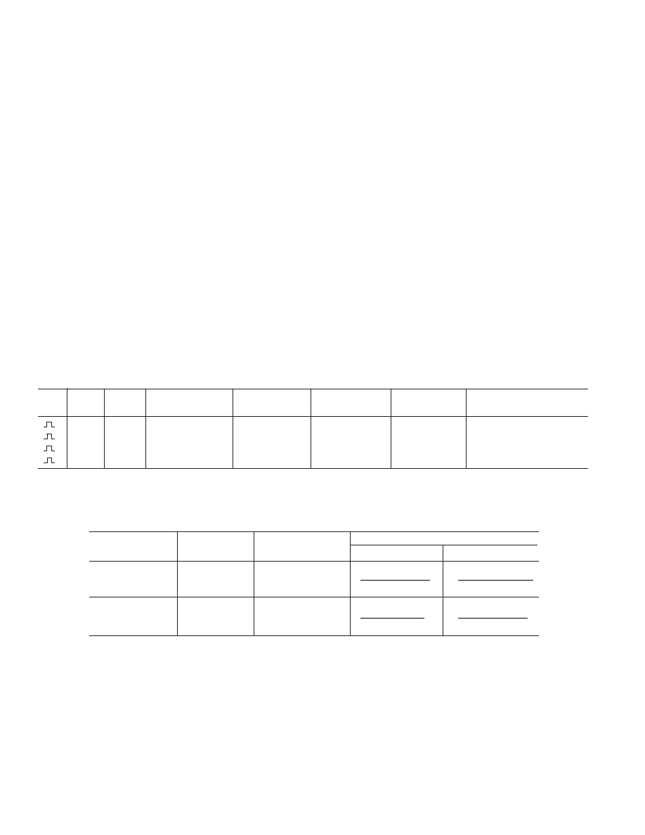
Table III. Calibration Truth Table
*
Calibration
Zero-Scale
Full-Scale
Calibration
CAL
SC1
SC2
Type
Calibration
Sequence
Time
00
Self-Calibration
VAGND
VREF
One Step
3,145,655 Clock Cycles
11
System Offset
AIN
First Step
1,052,599 Clock Cycles
01
System Gain
AIN
Second Step
1,068,813 Clock Cycles
10
System Offset
AIN
VREF
One Step
2,117,389 Clock Cycles
*DRDY remains high throughout the calibration sequence. In the Self-Calibration mode, DRDY falls once the AD7703 has settled to the analog input. In all other
modes,
DRDY falls as the device begins to settle.
Table IV. Output Code Size After Calibration
1 LSB
Calibration Mode
Zero Scale
Gain Factor
Unipolar
Bipolar
Self-Calibration
VAGND
VREF
(VREF –VAGND )
1048576
2(VREF –VAGND )
1048576
System Calibration
SOFF
SGAIN
(SGAIN – SOFF )
1048576
2(SGAIN – SOFF )
1048576
相关PDF资料 |
PDF描述 |
|---|---|
| LT1081CSW#TRPBF | IC DRVR/RCVR DL-RS232 5V 16SOIC |
| LT1081CSW#TR | IC TXRX DUAL RS232 5V LP 16SOIC |
| MS3100A22-23P | CONN RCPT 8POS WALL MNT W/PINS |
| LT1080CSW#TR | IC TXRX DUAL RS232 5V LP 18SOIC |
| IDT7205L12J8 | IC FIFO 4096X18 12NS 32PLCC |
相关代理商/技术参数 |
参数描述 |
|---|---|
| AD7703AR-REEL | 功能描述:IC ADC 20BIT LC2MOS MONO 20-SOIC RoHS:否 类别:集成电路 (IC) >> 数据采集 - 模数转换器 系列:- 标准包装:1 系列:- 位数:14 采样率(每秒):83k 数据接口:串行,并联 转换器数目:1 功率耗散(最大):95mW 电压电源:双 ± 工作温度:0°C ~ 70°C 安装类型:通孔 封装/外壳:28-DIP(0.600",15.24mm) 供应商设备封装:28-PDIP 包装:管件 输入数目和类型:1 个单端,双极 |
| AD7703ARZ | 功能描述:IC ADC 20BIT LC2MOS 20-SOIC RoHS:是 类别:集成电路 (IC) >> 数据采集 - 模数转换器 系列:- 标准包装:1 系列:- 位数:14 采样率(每秒):83k 数据接口:串行,并联 转换器数目:1 功率耗散(最大):95mW 电压电源:双 ± 工作温度:0°C ~ 70°C 安装类型:通孔 封装/外壳:28-DIP(0.600",15.24mm) 供应商设备封装:28-PDIP 包装:管件 输入数目和类型:1 个单端,双极 |
| AD7703BN | 功能描述:IC ADC 20BIT LC2MOS 20-DIP RoHS:否 类别:集成电路 (IC) >> 数据采集 - 模数转换器 系列:- 产品培训模块:Lead (SnPb) Finish for COTS Obsolescence Mitigation Program 标准包装:2,500 系列:- 位数:12 采样率(每秒):3M 数据接口:- 转换器数目:- 功率耗散(最大):- 电压电源:- 工作温度:- 安装类型:表面贴装 封装/外壳:SOT-23-6 供应商设备封装:SOT-23-6 包装:带卷 (TR) 输入数目和类型:- |
| AD7703BNZ | 功能描述:IC ADC 20BIT LC2MOS MONO 20DIP RoHS:是 类别:集成电路 (IC) >> 数据采集 - 模数转换器 系列:- 其它有关文件:TSA1204 View All Specifications 标准包装:1 系列:- 位数:12 采样率(每秒):20M 数据接口:并联 转换器数目:2 功率耗散(最大):155mW 电压电源:模拟和数字 工作温度:-40°C ~ 85°C 安装类型:表面贴装 封装/外壳:48-TQFP 供应商设备封装:48-TQFP(7x7) 包装:Digi-Reel® 输入数目和类型:4 个单端,单极;2 个差分,单极 产品目录页面:1156 (CN2011-ZH PDF) 其它名称:497-5435-6 |
| AD7703BQ | 制造商:AD 制造商全称:Analog Devices 功能描述:LC2MOS 20-Bit A/D Converter |
发布紧急采购,3分钟左右您将得到回复。