- 您现在的位置:买卖IC网 > PDF目录10097 > AD7703AR (Analog Devices Inc)IC ADC 20BIT LC2MOS 20-SOIC PDF资料下载
参数资料
| 型号: | AD7703AR |
| 厂商: | Analog Devices Inc |
| 文件页数: | 3/16页 |
| 文件大小: | 0K |
| 描述: | IC ADC 20BIT LC2MOS 20-SOIC |
| 标准包装: | 1 |
| 位数: | 20 |
| 采样率(每秒): | 4k |
| 数据接口: | 串行 |
| 转换器数目: | 1 |
| 功率耗散(最大): | 37mW |
| 电压电源: | 模拟和数字,双 ± |
| 工作温度: | -40°C ~ 85°C |
| 安装类型: | 表面贴装 |
| 封装/外壳: | 20-SOIC(0.295",7.50mm 宽) |
| 供应商设备封装: | 20-SOIC W |
| 包装: | 管件 |
| 输入数目和类型: | 1 个单端,单极;1 个单端,双极 |
REV. E
AD7703
–11–
Table V. Output Coding
Input Voltage, Unipolar Mode
Input Voltage, Bipolar Mode
System Calibration
Self-Calibration
Output Codes
Self-Calibration
System Calibration
>(SGAIN –1.5 LSB)
>(VREF – 1.5 LSB)
FFFFF
>(VREF –1.5 LSB)
>(SGAIN – 1.5 LSB)
SGAIN – 1.5 LSB
VREF – 1.5 LSB
FFFFF
FFFFE
VREF – 1.5 LSB
SGAIN – 1.5 LSB
(SGAIN – SOFF)/2 – 0.5 LSB
(VREF – VAGND)/2 – 0.5 LSB
80000
7FFFF
VAGND – 0.5 LSB
SOFF – 0.5 LSB
SOFF + 0.5 LSB
VAGND + 0.5 LSB
00001
00000
–VREF + 0.5 LSB
–SGAIN + 2 SOFF + 0.5 LSB
<(SOFF + 0.5 LSB)
<(VAGND + 0.5 LSB)
00000
<(–VREF + 0.5 LSB)
<(–SGAIN +2 SOFF + 0.5 LSB)
In the Bipolar mode, the system offset calibration range is
restricted to ±0.4 VREF. It should be noted that the span restric-
tions limit the amount of offset that can be calibrated. The span
range of the converter in Bipolar mode is equidistant around the
voltage used for the zero-scale point. When the zero-scale point
is calibrated, it must not cause either of the two endpoints of the
bipolar transfer function to exceed the positive or the negative
input overrange points (+VREF + 0.1) V or (–VREF + 0.1) V. If
the span range is set to a minimum (0.8 VREF), the offset voltage
can move +0.4 VREF without causing the endpoints of the trans-
fer function to exceed the overrange points. Alternatively, if the
span range is set to 2VREF, the input offset cannot move more
than +0.1 V or –0.1 V before an endpoint of the transfer func-
tion exceeds the input overrange limit.
POWER-UP AND CALIBRATION
A calibration cycle must be carried out after power-up to initial-
ize the device to a consistent starting condition and correct
calibration. The CAL pin must be held high for at least four
clock cycles, after which calibration is initiated on the falling
edge of CAL and takes a maximum of 3,145,655 clock cycles
(approximately 768 ms with a 4.096 MHz clock). See Table III.
The type of calibration cycle initiated by CAL is determined by
the SC1 and SC2 inputs, in accordance with Table III.
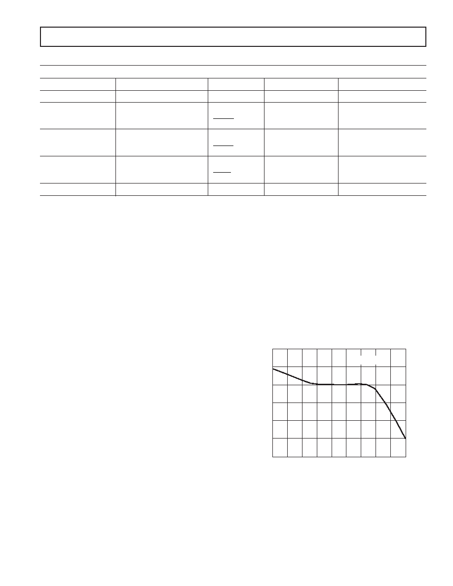
Drift Considerations
The AD7703 uses chopper stabilization techniques to minimize
input offset drift. Charge injection in the analog switches and
leakage currents at the sampling node are the primary sources of
offset voltage drift in the converter. Figure 13 indicates the typical
offset due to temperature changes after calibration at 25°C. Drift
is relatively flat up to 75°C. Above this temperature, leakage
current becomes the main source of offset drift. Since leakage
current doubles approximately every 10°C, the offset drifts
accordingly. The value of the voltage on the sample capacitor is
updated at a rate determined by the master clock; therefore, the
amount of offset drift that occurs will be proportional to the
elapsed time between samples. Thus, to minimize offset drift at
higher temperatures, higher CLKIN rates are recommended.
Gain drift within the converter depends mainly upon the tem-
perature tracking of the internal capacitors. It is not affected by
leakage currents so it is significantly less than offset drift. The
typical gain drift of the AD7703 is less than 40 LSB over the
specified temperature range.
Measurement errors due to offset drift or gain drift can be
eliminated at any time by recalibrating the converter. Using the
system calibration mode can also minimize offset and gain errors
in the signal conditioning circuitry. Integral and differential
linearity are not significantly affected by temperature changes.
BIPOLAR
OFFSET
–
LSBs
160
0
–80
–160
–240
–320
–55
5
25
105
125
TEMPERATURE – C
80
–35
–15
45
65
85
CLKIN = 4.096MHz
Figure 13. Typical Bipolar Offset vs. Temperature
after Calibration at 25°C
相关PDF资料 |
PDF描述 |
|---|---|
| LT1081CSW#TRPBF | IC DRVR/RCVR DL-RS232 5V 16SOIC |
| LT1081CSW#TR | IC TXRX DUAL RS232 5V LP 16SOIC |
| MS3100A22-23P | CONN RCPT 8POS WALL MNT W/PINS |
| LT1080CSW#TR | IC TXRX DUAL RS232 5V LP 18SOIC |
| IDT7205L12J8 | IC FIFO 4096X18 12NS 32PLCC |
相关代理商/技术参数 |
参数描述 |
|---|---|
| AD7703AR-REEL | 功能描述:IC ADC 20BIT LC2MOS MONO 20-SOIC RoHS:否 类别:集成电路 (IC) >> 数据采集 - 模数转换器 系列:- 标准包装:1 系列:- 位数:14 采样率(每秒):83k 数据接口:串行,并联 转换器数目:1 功率耗散(最大):95mW 电压电源:双 ± 工作温度:0°C ~ 70°C 安装类型:通孔 封装/外壳:28-DIP(0.600",15.24mm) 供应商设备封装:28-PDIP 包装:管件 输入数目和类型:1 个单端,双极 |
| AD7703ARZ | 功能描述:IC ADC 20BIT LC2MOS 20-SOIC RoHS:是 类别:集成电路 (IC) >> 数据采集 - 模数转换器 系列:- 标准包装:1 系列:- 位数:14 采样率(每秒):83k 数据接口:串行,并联 转换器数目:1 功率耗散(最大):95mW 电压电源:双 ± 工作温度:0°C ~ 70°C 安装类型:通孔 封装/外壳:28-DIP(0.600",15.24mm) 供应商设备封装:28-PDIP 包装:管件 输入数目和类型:1 个单端,双极 |
| AD7703BN | 功能描述:IC ADC 20BIT LC2MOS 20-DIP RoHS:否 类别:集成电路 (IC) >> 数据采集 - 模数转换器 系列:- 产品培训模块:Lead (SnPb) Finish for COTS Obsolescence Mitigation Program 标准包装:2,500 系列:- 位数:12 采样率(每秒):3M 数据接口:- 转换器数目:- 功率耗散(最大):- 电压电源:- 工作温度:- 安装类型:表面贴装 封装/外壳:SOT-23-6 供应商设备封装:SOT-23-6 包装:带卷 (TR) 输入数目和类型:- |
| AD7703BNZ | 功能描述:IC ADC 20BIT LC2MOS MONO 20DIP RoHS:是 类别:集成电路 (IC) >> 数据采集 - 模数转换器 系列:- 其它有关文件:TSA1204 View All Specifications 标准包装:1 系列:- 位数:12 采样率(每秒):20M 数据接口:并联 转换器数目:2 功率耗散(最大):155mW 电压电源:模拟和数字 工作温度:-40°C ~ 85°C 安装类型:表面贴装 封装/外壳:48-TQFP 供应商设备封装:48-TQFP(7x7) 包装:Digi-Reel® 输入数目和类型:4 个单端,单极;2 个差分,单极 产品目录页面:1156 (CN2011-ZH PDF) 其它名称:497-5435-6 |
| AD7703BQ | 制造商:AD 制造商全称:Analog Devices 功能描述:LC2MOS 20-Bit A/D Converter |
发布紧急采购,3分钟左右您将得到回复。