- 您现在的位置:买卖IC网 > PDF目录10744 > AD7730BRU-REEL7 (Analog Devices Inc)IC ADC TRANSDUCER BRIDGE 24TSSOP PDF资料下载
参数资料
| 型号: | AD7730BRU-REEL7 |
| 厂商: | Analog Devices Inc |
| 文件页数: | 19/53页 |
| 文件大小: | 0K |
| 描述: | IC ADC TRANSDUCER BRIDGE 24TSSOP |
| 标准包装: | 1,000 |
| 位数: | 24 |
| 通道数: | 1 |
| 功率(瓦特): | 125mW |
| 电压 - 电源,模拟: | 4.75 V ~ 5.25 V |
| 电压 - 电源,数字: | 2.7 V ~ 5.25 V |
| 封装/外壳: | 24-TSSOP(0.173",4.40mm 宽) |
| 供应商设备封装: | 24-TSSOP |
| 包装: | 带卷 (TR) |
| 配用: | EVAL-AD7730LEBZ-ND - BOARD EVALUATION FOR AD7730 EVAL-AD7730EBZ-ND - BOARD EVAL FOR AD7730 |
第1页第2页第3页第4页第5页第6页第7页第8页第9页第10页第11页第12页第13页第14页第15页第16页第17页第18页当前第19页第20页第21页第22页第23页第24页第25页第26页第27页第28页第29页第30页第31页第32页第33页第34页第35页第36页第37页第38页第39页第40页第41页第42页第43页第44页第45页第46页第47页第48页第49页第50页第51页第52页第53页
AD7730/AD7730L
–26–
If the AD7730 is performing either an offset or gain calibration
and the NOREF bit becomes active, the updating of the respec-
tive calibration register is inhibited to avoid loading incorrect
coefficients to this register. If the user is concerned about verify-
ing that a valid reference is in place every time a calibration is
performed, then the status of the NOREF bit should be checked
at the end of the calibration cycle.
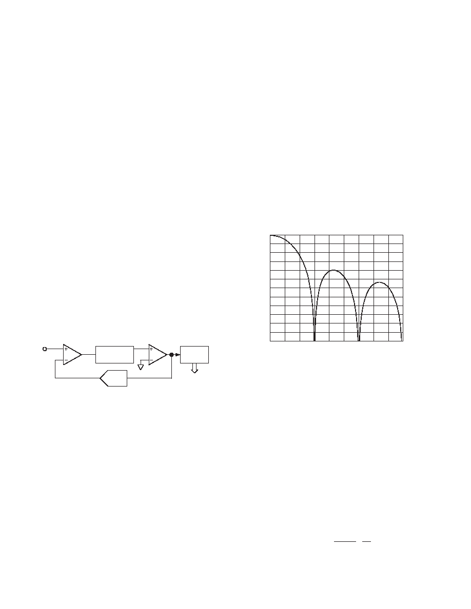
SIGMA-DELTA MODULATOR
A sigma-delta ADC generally consists of two main blocks, an
analog modulator and a digital filter. In the case of the AD7730,
the analog modulator consists of a difference amplifier, an inte-
grator block, a comparator and a feedback DAC as illustrated in
Figure 9. In operation, the analog signal sample is fed to the
difference amplifier along with the output of the feedback DAC.
The difference between these two signals is integrated and fed to
the comparator. The output of the comparator provides the
input to the feedback DAC so that the system functions as a
negative feedback loop that tries to minimize the difference
signal. The digital data that represents the analog input voltage
is contained in the duty cycle of the pulse train appearing at the
output of the comparator. This duty cycle data can be recovered
as a data word using the digital filter. The sampling frequency of
the modulator loop is many times higher than the bandwidth of
the input signal. The integrator in the modulator shapes the
quantization noise (which results from the analog-to-digital
conversion) so that the noise is pushed toward one half of the
modulator frequency. The digital filter then bandlimits the re-
sponse to a frequency significantly lower than one half of the
modulator frequency. In this manner, the 1-bit output of the
comparator is translated into a bandlimited, low noise output
from the AD7730.
DAC
INTEGRATOR
ANALOG
INPUT
DIFFERENCE
AMP
COMPARATOR
DIGITAL
FILTER
DIGITAL DATA
Figure 9. Sigma-Delta Modulator Block Diagram
DIGITAL FILTERING
Filter Architecture
The output of the modulator feeds directly into the digital filter.
This digital filter consists of two portions, a first stage filter and
a second stage filter. The first stage filter is a sinc3, low-pass
filter. The cutoff frequency and output rate of this first stage
filter is programmable. The second stage filter has three distinct
modes of operation. In its normal mode, it provides a low-pass
FIR filter that processes the output of the first stage filter. When
a step change is detected on the analog input, this second stage
filter enters a second mode where it performs a variable number
of averages for some time after the step change and then the
second stage filter switches back to the FIR filter. The third
option for the second stage filter is that it is completely bypassed
so the only filtering provided on the AD7730 is the first stage.
The various filter stages and options are discussed in the follow-
ing sections.
First Stage Filter
The first stage filter is a low-pass, sinc3 or (sinx/x)3 filter whose
primary function is to remove the quantization noise introduced
at the modulator. The cutoff frequency and output rate of this
filter is programmed via the SF0 to SF11 bits of the Filter Reg-
ister. The frequency response for this first stage filter is shown in
Figure 10. The response of this first stage filter is similar to that
of an averaging filter but with a sharper roll-off. The output rate
for the filter corresponds with the positioning of the first notch
of the filter’s frequency response. Thus, for the plot of Figure 10,
where the output rate is 600 Hz (fCLK IN = 4.9152 MHz and
SF = 512), the first notch of the filter is at 600 Hz. The notches
of this sinc3 filter are repeated at multiples of the first notch. The
filter provides attenuation of better than 100 dB at these notches.
Programming a different cutoff frequency via SF0 – SF11 does
not alter the profile of the filter response; it changes the fre-
quency of the notches as outlined in the Filter Registers section.
This response is repeated at either side of the input sampling
frequency (307 kHz) and at either side of multiples of the input
sampling frequency.
FREQUENCY – Hz
0
–60
–100
0
1800
GAIN
–
dB
200
400
600
800
1000
1200 1400
1600
–10
–50
–70
–90
–30
–40
–80
–20
–120
–110
Figure 10. Frequency Response of First Stage Filter
The first stage filter has two basic modes of operation. The
primary mode of operation for weigh-scale applications is chop
mode, which is achieved by placing a 1 in the CHP bit of the
Filter Register. The part should be operated in this mode when
drift and noise rejection are important criteria in the application.
The alternative mode of operation is the nonchop mode, with
CHP at 0, which would be used when higher throughput rates
are a concern or in applications where the reduced rejection at
the chopping frequency in chop mode is an issue.
Nonchop Mode
With chop mode disabled on the AD7730, the first stage filter
continuously processes input data and produces a result at an
output rate determined by the SF word. Operating in nonchop
mode can result in a 20% reduction in noise for a given band-
width, but without the excellent drift and noise rejection ben-
efits which accrue from chopping the part. The output update
and first notch of this first stage filter correspond and are deter-
mined by the relationship:
Output Rate
=
f CLK IN
16
×
1
SF
where SF is the decimal equivalent of the data loaded to the SF
bits of the Filter Register and fCLK IN is the master clock frequency.
REV. B
相关PDF资料 |
PDF描述 |
|---|---|
| AD7730BRU-REEL | IC ADC TRANSDUCER BRIDGE 24TSSOP |
| AD7730BR-REEL | IC ADC TRANSDUCER BRIDGE 24-SOIC |
| AD7730LBR-REEL7 | IC ADC TRANSDUCER BRIDGE 24SOIC |
| XRD9824ACD-F | IC 14B CCD/CIS SIG PROC 20SOIC |
| MAX933CSA+ | IC COMPARATOR W/REF 8-SOIC |
相关代理商/技术参数 |
参数描述 |
|---|---|
| AD7730BRUZ | 功能描述:IC ADC TRANSDUCER BRIDGE 24TSSOP RoHS:是 类别:集成电路 (IC) >> 数据采集 - 模拟前端 (AFE) 系列:- 产品培训模块:Lead (SnPb) Finish for COTS Obsolescence Mitigation Program 标准包装:2,500 系列:- 位数:- 通道数:2 功率(瓦特):- 电压 - 电源,模拟:3 V ~ 3.6 V 电压 - 电源,数字:3 V ~ 3.6 V 封装/外壳:32-VFQFN 裸露焊盘 供应商设备封装:32-QFN(5x5) 包装:带卷 (TR) |
| AD7730BRUZ-REEL | 功能描述:IC ADC BRIDGE TRANSDUCER 24TSSOP RoHS:是 类别:集成电路 (IC) >> 数据采集 - 模拟前端 (AFE) 系列:- 产品培训模块:Lead (SnPb) Finish for COTS Obsolescence Mitigation Program 标准包装:2,500 系列:- 位数:- 通道数:2 功率(瓦特):- 电压 - 电源,模拟:3 V ~ 3.6 V 电压 - 电源,数字:3 V ~ 3.6 V 封装/外壳:32-VFQFN 裸露焊盘 供应商设备封装:32-QFN(5x5) 包装:带卷 (TR) |
| AD7730BRUZ-REEL7 | 功能描述:IC ADC BRIDGE TRANSDUCER 24TSSOP RoHS:是 类别:集成电路 (IC) >> 数据采集 - 模拟前端 (AFE) 系列:- 产品培训模块:Lead (SnPb) Finish for COTS Obsolescence Mitigation Program 标准包装:2,500 系列:- 位数:- 通道数:2 功率(瓦特):- 电压 - 电源,模拟:3 V ~ 3.6 V 电压 - 电源,数字:3 V ~ 3.6 V 封装/外壳:32-VFQFN 裸露焊盘 供应商设备封装:32-QFN(5x5) 包装:带卷 (TR) |
| AD7730BRZ | 功能描述:IC ADC BRIDGE TRANSDUCER 24-SOIC RoHS:是 类别:集成电路 (IC) >> 数据采集 - 模拟前端 (AFE) 系列:- 产品培训模块:Lead (SnPb) Finish for COTS Obsolescence Mitigation Program 标准包装:2,500 系列:- 位数:- 通道数:2 功率(瓦特):- 电压 - 电源,模拟:3 V ~ 3.6 V 电压 - 电源,数字:3 V ~ 3.6 V 封装/外壳:32-VFQFN 裸露焊盘 供应商设备封装:32-QFN(5x5) 包装:带卷 (TR) |
| AD7730BRZ | 制造商:Analog Devices 功能描述:IC, ADC, 24BIT, 1.2KSPS, SOIC-24 |
发布紧急采购,3分钟左右您将得到回复。