- 您现在的位置:买卖IC网 > PDF目录10243 > AD7853LARS-REEL (Analog Devices Inc)IC ADC 12BIT SRL 200KSPS 24-SSOP PDF资料下载
参数资料
| 型号: | AD7853LARS-REEL |
| 厂商: | Analog Devices Inc |
| 文件页数: | 11/34页 |
| 文件大小: | 0K |
| 描述: | IC ADC 12BIT SRL 200KSPS 24-SSOP |
| 标准包装: | 1,500 |
| 位数: | 12 |
| 采样率(每秒): | 100k |
| 数据接口: | 8051,QSPI?,串行,SPI? µP |
| 转换器数目: | 2 |
| 功率耗散(最大): | 33mW |
| 电压电源: | 模拟和数字 |
| 工作温度: | -40°C ~ 85°C |
| 安装类型: | 表面贴装 |
| 封装/外壳: | 24-SSOP(0.209",5.30mm 宽) |
| 供应商设备封装: | 24-SSOP |
| 包装: | 带卷 (TR) |
| 输入数目和类型: | 1 个伪差分,单极;1 个伪差分,双极 |
第1页第2页第3页第4页第5页第6页第7页第8页第9页第10页当前第11页第12页第13页第14页第15页第16页第17页第18页第19页第20页第21页第22页第23页第24页第25页第26页第27页第28页第29页第30页第31页第32页第33页第34页
REV. B
–19–
AD7853/AD7853L
Table VI. Power Management Options
PMGT1 PMGT0
SLEEP
Bit
Pin
Comment
00
0
Full Power-Down if Not Cali-
brating or Converting (Default
Condition After Power-On)
00
1
Normal Operation
01
X
Normal Operation
(Independent of the
SLEEP Pin)
10
X
Full Power-Down
11
X
Partial Power-Down if Not
Converting
POWER-UP TIMES
Using an External Reference
When the AD7853 is powered up, the part is powered up from
one of two conditions. First, when the power supplies are ini-
tially powered up and, secondly, when the part is powered up
from either a hardware or software power-down (see last section).
When AVDD and DVDD are powered up, the AD7853 should be
left idle for approximately 32 ms (4 MHz CLK) to allow for the
autocalibration if a 10 nF cap is placed on the
CAL pin, (see
Calibration section). During power-up the functionality of the
SLEEP pin is disabled, i.e., the part will not power down until
the end of the calibration if
SLEEP is tied logic low. The auto-
calibration on power-up can be disabled if the
CAL pin is tied to
a logic high. If the autocalibration is disabled, then the user must
take into account the time required by the AD7853 to power-up
before a self-calibration is carried out. This power-up time is the
time taken for the AD7853 to power up when power is first
applied (300
s) typ) or the time it takes the external reference
to settle to the 12-bit level–whichever is the longer.
The AD7853 powers up from a full hardware or software
power-down in 5
s typ. This limits the throughput which the
part is capable of to 104 kSPS for the AD7853 operating with a
4 MHz CLK and 66 kSPS for the AD7853L with a 1.8 MHz
CLK when powering down between conversions. Figure 24
shows how power-down between conversions is implemented
using the
CONVST pin. The user first selects the power-down
between conversions option by using the
SLEEP pin and the
power management bits, PMGT1 and PMGT0, in the control
register, (see last section). In this mode the AD7853 automati-
cally enters a full power-down at the end of a conversion, i.e.,
when BUSY goes low. The falling edge of the next
CONVST
pulse causes the part to power up. Assuming the external refer-
ence is left powered up, the AD7853 should be ready for normal
operation 5
s after this falling edge. The rising edge of CONVST
initiates a conversion so the
CONVST pulse should be at least
5
s wide. The part automatically powers down on completion
of the conversion.
NOTE: Where the software CONVST is used or automatic
full power-down, the part must be powered up in software with
an extra write setting PMGT1 = 0 and PMGT0 = 1 before a
conversion is initiated in the next write. Automatic partial power-
down after a calibration is not possible; the part must be powered
down manually. If software calibrations are to be used when
operating in the partial power-down mode, then three separate
writes are required. The first initiates the type of calibration
required, the second write powers the part down into partial
power-down mode, while the third write powers the part up
again before the next calibration command is issued.
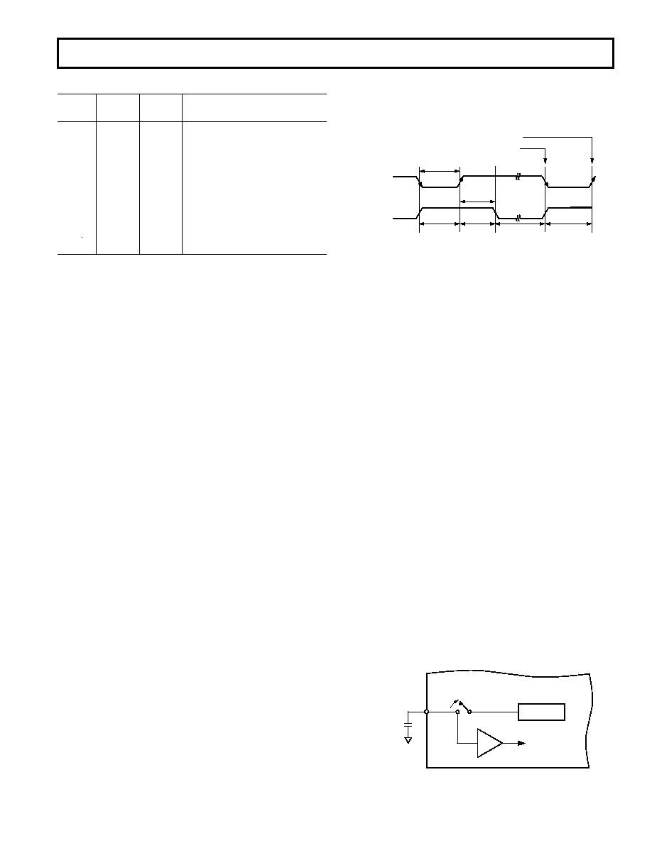
5 s
tCONVERT
POWER-UP
TIME
NORMAL
OPERATION
FULL
POWER-DOWN
POWER-UP
TIME
START CONVERSION ON RISING EDGE
POWER-UP ON FALLING EDGE
CONVST
BUSY
Figure 24. Power-Up Timing When Using
CONVST Pin
Using the Internal (On-Chip) Reference
As in the case of an external reference, the AD7853 can power-
up from one of two conditions, power-up after the supplies are
connected or power-up from hardware/software power-down.
When using the on-chip reference and powering up when AVDD
and DVDD are first connected, it is recommended that the power-
up calibration mode be disabled as explained above. When using
the on-chip reference, the power-up time is effectively the time
it takes to charge up the external capacitor on the REFIN/REFOUT
pin. This time is given by the equation:
tUP = 9 × R × C
where R
150 k and C = external capacitor.
The recommended value of the external capacitor is 100 nF;
this gives a power-up time of approximately 135 ms before a
calibration is initiated and normal operation should commence.
When CREF is fully charged, the power-up time from a hardware
or software power-down reduces to 5
s. This is because an
internal switch opens to provide a high impedance discharge
path for the reference capacitor during power-down—see Figure
23. An added advantage of the low charge leakage from the
reference capacitor during power-down is that even though the
reference is being powered down between conversions, the
reference capacitor holds the reference voltage to within
0.5 LSBs with throughput rates of 100 samples/second and over
with a full power-down between conversions. A high input im-
pedance op amp like the AD707 should be used to buffer this
reference capacitor if it is being used externally. Note, if the
AD7853 is left in its power-down state for more than 100 ms,
the charge on CREF will start to leak away and the power-up
time will increase. If this long power-up time is a problem, the
user can use a partial power-down for the last conversion so the
reference remains powered up.
AD7853
REFIN/REFOUT
EXTERNAL
CAPACITOR
SWITCH OPENS
DURING POWER-DOWN
BUF
ON-CHIP
REFERENCE
TO OTHER
CIRCUITRY
Figure 25. On-Chip Reference During Power-Down
相关PDF资料 |
PDF描述 |
|---|---|
| VE-23T-CU-F4 | CONVERTER MOD DC/DC 6.5V 200W |
| VE-B2M-MW-F4 | CONVERTER MOD DC/DC 10V 100W |
| VI-26F-MY | CONVERTER MOD DC/DC 72V 50W |
| VE-B2M-MW-F3 | CONVERTER MOD DC/DC 10V 100W |
| VE-23R-IW-S | CONVERTER MOD DC/DC 7.5V 100W |
相关代理商/技术参数 |
参数描述 |
|---|---|
| AD7853LARSZ | 功能描述:IC ADC 12BIT SRL 200KSPS 24SSOP RoHS:是 类别:集成电路 (IC) >> 数据采集 - 模数转换器 系列:- 标准包装:1,000 系列:- 位数:12 采样率(每秒):300k 数据接口:并联 转换器数目:1 功率耗散(最大):75mW 电压电源:单电源 工作温度:0°C ~ 70°C 安装类型:表面贴装 封装/外壳:24-SOIC(0.295",7.50mm 宽) 供应商设备封装:24-SOIC 包装:带卷 (TR) 输入数目和类型:1 个单端,单极;1 个单端,双极 |
| AD7853LARSZ-REEL | 功能描述:IC ADC 12BIT SRL 200KSPS 24SSOP RoHS:是 类别:集成电路 (IC) >> 数据采集 - 模数转换器 系列:- 标准包装:1,000 系列:- 位数:16 采样率(每秒):45k 数据接口:串行 转换器数目:2 功率耗散(最大):315mW 电压电源:模拟和数字 工作温度:0°C ~ 70°C 安装类型:表面贴装 封装/外壳:28-SOIC(0.295",7.50mm 宽) 供应商设备封装:28-SOIC W 包装:带卷 (TR) 输入数目和类型:2 个单端,单极 |
| AD7853LARZ | 功能描述:IC ADC 12BIT SRL 200KSPS 24SOIC RoHS:是 类别:集成电路 (IC) >> 数据采集 - 模数转换器 系列:- 标准包装:1,000 系列:- 位数:12 采样率(每秒):300k 数据接口:并联 转换器数目:1 功率耗散(最大):75mW 电压电源:单电源 工作温度:0°C ~ 70°C 安装类型:表面贴装 封装/外壳:24-SOIC(0.295",7.50mm 宽) 供应商设备封装:24-SOIC 包装:带卷 (TR) 输入数目和类型:1 个单端,单极;1 个单端,双极 |
| AD7853LARZ-REEL | 功能描述:IC ADC 12BIT SRL 200KSPS 24SOIC RoHS:是 类别:集成电路 (IC) >> 数据采集 - 模数转换器 系列:- 产品培训模块:Lead (SnPb) Finish for COTS Obsolescence Mitigation Program 标准包装:2,500 系列:- 位数:12 采样率(每秒):3M 数据接口:- 转换器数目:- 功率耗散(最大):- 电压电源:- 工作温度:- 安装类型:表面贴装 封装/外壳:SOT-23-6 供应商设备封装:SOT-23-6 包装:带卷 (TR) 输入数目和类型:- |
| AD7853LBN | 功能描述:IC ADC 12BIT SRL 200KSPS 24-DIP RoHS:否 类别:集成电路 (IC) >> 数据采集 - 模数转换器 系列:- 标准包装:1,000 系列:- 位数:12 采样率(每秒):300k 数据接口:并联 转换器数目:1 功率耗散(最大):75mW 电压电源:单电源 工作温度:0°C ~ 70°C 安装类型:表面贴装 封装/外壳:24-SOIC(0.295",7.50mm 宽) 供应商设备封装:24-SOIC 包装:带卷 (TR) 输入数目和类型:1 个单端,单极;1 个单端,双极 |
发布紧急采购,3分钟左右您将得到回复。