- 您现在的位置:买卖IC网 > PDF目录10243 > AD7853LARS-REEL (Analog Devices Inc)IC ADC 12BIT SRL 200KSPS 24-SSOP PDF资料下载
参数资料
| 型号: | AD7853LARS-REEL |
| 厂商: | Analog Devices Inc |
| 文件页数: | 19/34页 |
| 文件大小: | 0K |
| 描述: | IC ADC 12BIT SRL 200KSPS 24-SSOP |
| 标准包装: | 1,500 |
| 位数: | 12 |
| 采样率(每秒): | 100k |
| 数据接口: | 8051,QSPI?,串行,SPI? µP |
| 转换器数目: | 2 |
| 功率耗散(最大): | 33mW |
| 电压电源: | 模拟和数字 |
| 工作温度: | -40°C ~ 85°C |
| 安装类型: | 表面贴装 |
| 封装/外壳: | 24-SSOP(0.209",5.30mm 宽) |
| 供应商设备封装: | 24-SSOP |
| 包装: | 带卷 (TR) |
| 输入数目和类型: | 1 个伪差分,单极;1 个伪差分,双极 |
第1页第2页第3页第4页第5页第6页第7页第8页第9页第10页第11页第12页第13页第14页第15页第16页第17页第18页当前第19页第20页第21页第22页第23页第24页第25页第26页第27页第28页第29页第30页第31页第32页第33页第34页
REV. B
–26–
AD7853/AD7853L
The most important point about these two modes of operation
mode is that the result of the current conversion is clocked
out during the same conversion and a write to the part dur-
ing this conversion is for the next conversion. The arrangement
is shown in Figure 37. Figure 38 and Figure 39 show more
detailed timing for the arrangement of Figure 37.
WRITE N+1
CONVERSION N
READ N
5 s
WRITE N+2
CONVERSION N+1
READ N+1
WRITE N+3
CONVERSION N+2
READ N+2
5 s
THE CONVERSION RESULT DUE TO
WRITE N+1 IS READ HERE
5 s
Figure 37.
t
1
CONVST
(I/P)
SCLK
(O/P)
CONVERSION ENDS
4.6 s LATER
SERIAL READ
AND WRITE
OPERATIONS
OUTPUT SERIAL SHIFT
REGISTER IS RESET
READ OPERATION
SHOULD END 500ns
PRIOR TO NEXT RISING
400ns MIN
BUSY
(O/P)
SYNC
(O/P)
CONVERSION IS INITIATED
AND TRACK/HOLD GOES
INTO HOLD
EDGE OF
CONVST
t
1 = 100ns MIN
t
CONVERT = 4.6 s
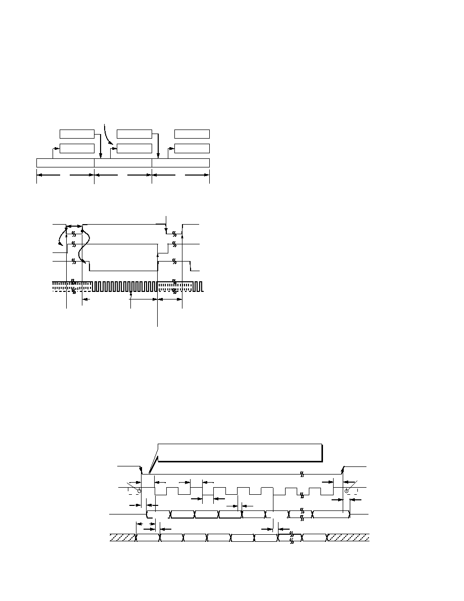
Figure 38. Mode 4, 5 Timing Diagram (SM1 = 1, SM2 = 1
and 0)
In Figure 38 the first point to note is that the BUSY,
SYNC,
and SCLK are all outputs from the AD7853/AD7853L with the
CONVST being the only input signal. Conversion is initiated
with the
CONVST signal going low. This CONVST falling
edge also triggers the BUSY to go high. The
CONVST signal
rising edge triggers the
SYNC to go low after a short delay
(0.5 tCLKIN to 1.5 tCLKIN typically) after which the SCLK will
clock out the data on the DOUT pin during conversion. The
data on the DIN pin is also clocked in to the AD7853/AD7853L
by the same SCLK for the next conversion. The read/write
operations must be complete after sixteen clock cycles (which
takes 4.6
s approximately from the rising edge of CONVST assum-
ing a 4 MHz CLKIN). At this time the conversion will be com-
plete, the
SYNC will go high, and the BUSY will go low. The
next falling edge of the
CONVST must occur at least 400 ns
after the falling edge of BUSY to allow the track/hold amplifier
adequate acquisition time as shown in Figure 38. This gives a
throughput time of 5
s. The maximum throughput rate in this
case is 200 kHz (AD7853) and 100 kHz (AD7853L).
In these interface modes the part is now the master and the DSP
is the slave. Figure 39 is an expansion of Figure 38. The
AD7853/AD7853L will ensure
SYNC goes low after the rising
edge C of the continuous SCLK (Interface Mode 5) in Figure
39. Only in the case of a noncontinuous SCLK (Interface Mode
4) will the time t4 apply. The first data bit is clocked out from
the falling edge of
SYNC. The SCLK rising edge clocks out all
subsequent bits on the DOUT pin. The input data present on
the DIN pin is clocked in on the rising edge of the SCLK. The
POLARITY pin may be used to change the SCLK edge which
the data is sampled on and clocked out on. The
SYNC will go
high after the 16th SCLK rising edge and before the falling edge
D of the continuous SCLK in Figure 39. This ensures the part
will not clock in an extra bit from the DIN pin or clock out an
extra bit on the DOUT pin.
If the user has control of the
CONVST pin but does not want to
exercise it for every conversion, the control register may be used
to start a conversion. Setting the CONVST bit in the control
register to 1 starts a conversion. If the user does not have con-
trol of the
CONVST pin, a conversion should not be initiated
by writing to the control register. The reason for this is that the
user may get “locked out” and not be able to perform any fur-
ther write/read operations. When a conversion is started by
writing to the control register, the
SYNC goes low and read/
write operations take place while the conversion is in progress.
However, once the conversion is complete, there is no way of
writing to the part unless the
CONVST pin is exercised. The
CONVST signal triggers the SYNC signal low which allows
read/write operations to take place.
SYNC must be low to per-
form read/write operations. The
SYNC is triggered low by the
CONVST signal rising edge or setting the CONVST bit in the
control register to 1. Therefore if there is not full control of the
CONVST pin the user may end up getting “locked out.”
DOUT (O/P)
SCLK (O/P)
SYNC (O/P)
DIN (I/P)
t
8
POLARITY PIN
LOGIC HIGH
1
23
4
5
6
16
DB0
DB15
DB14
DB13
DB12
DB11
DB10
DB0
THREE-
STATE
THREE-
STATE
DB11
DB10
DB14
DB13
DB12
t
6
t
10
t
9
t
12
t
11A
t
4
t
5
DB15
t
8
t
7
C
D
t
4 = 0.6tSCLK (NONCONTINUOUS SCLK), t6 = 75/115 MAX (5V/3V),
t
7 = 40/60ns MIN (5V/3V), t8 = 20/30 MIN (5V/3V), t11A = 50ns MAX
Figure 39. Timing Diagram for Read/Write with
SYNC Output and SCLK Output (Continuous and Noncontinuous)
(i.e., Operating Mode Numbers 4 and 5, SM1 = 1, SM2 = 1 and 0)
相关PDF资料 |
PDF描述 |
|---|---|
| VE-23T-CU-F4 | CONVERTER MOD DC/DC 6.5V 200W |
| VE-B2M-MW-F4 | CONVERTER MOD DC/DC 10V 100W |
| VI-26F-MY | CONVERTER MOD DC/DC 72V 50W |
| VE-B2M-MW-F3 | CONVERTER MOD DC/DC 10V 100W |
| VE-23R-IW-S | CONVERTER MOD DC/DC 7.5V 100W |
相关代理商/技术参数 |
参数描述 |
|---|---|
| AD7853LARSZ | 功能描述:IC ADC 12BIT SRL 200KSPS 24SSOP RoHS:是 类别:集成电路 (IC) >> 数据采集 - 模数转换器 系列:- 标准包装:1,000 系列:- 位数:12 采样率(每秒):300k 数据接口:并联 转换器数目:1 功率耗散(最大):75mW 电压电源:单电源 工作温度:0°C ~ 70°C 安装类型:表面贴装 封装/外壳:24-SOIC(0.295",7.50mm 宽) 供应商设备封装:24-SOIC 包装:带卷 (TR) 输入数目和类型:1 个单端,单极;1 个单端,双极 |
| AD7853LARSZ-REEL | 功能描述:IC ADC 12BIT SRL 200KSPS 24SSOP RoHS:是 类别:集成电路 (IC) >> 数据采集 - 模数转换器 系列:- 标准包装:1,000 系列:- 位数:16 采样率(每秒):45k 数据接口:串行 转换器数目:2 功率耗散(最大):315mW 电压电源:模拟和数字 工作温度:0°C ~ 70°C 安装类型:表面贴装 封装/外壳:28-SOIC(0.295",7.50mm 宽) 供应商设备封装:28-SOIC W 包装:带卷 (TR) 输入数目和类型:2 个单端,单极 |
| AD7853LARZ | 功能描述:IC ADC 12BIT SRL 200KSPS 24SOIC RoHS:是 类别:集成电路 (IC) >> 数据采集 - 模数转换器 系列:- 标准包装:1,000 系列:- 位数:12 采样率(每秒):300k 数据接口:并联 转换器数目:1 功率耗散(最大):75mW 电压电源:单电源 工作温度:0°C ~ 70°C 安装类型:表面贴装 封装/外壳:24-SOIC(0.295",7.50mm 宽) 供应商设备封装:24-SOIC 包装:带卷 (TR) 输入数目和类型:1 个单端,单极;1 个单端,双极 |
| AD7853LARZ-REEL | 功能描述:IC ADC 12BIT SRL 200KSPS 24SOIC RoHS:是 类别:集成电路 (IC) >> 数据采集 - 模数转换器 系列:- 产品培训模块:Lead (SnPb) Finish for COTS Obsolescence Mitigation Program 标准包装:2,500 系列:- 位数:12 采样率(每秒):3M 数据接口:- 转换器数目:- 功率耗散(最大):- 电压电源:- 工作温度:- 安装类型:表面贴装 封装/外壳:SOT-23-6 供应商设备封装:SOT-23-6 包装:带卷 (TR) 输入数目和类型:- |
| AD7853LBN | 功能描述:IC ADC 12BIT SRL 200KSPS 24-DIP RoHS:否 类别:集成电路 (IC) >> 数据采集 - 模数转换器 系列:- 标准包装:1,000 系列:- 位数:12 采样率(每秒):300k 数据接口:并联 转换器数目:1 功率耗散(最大):75mW 电压电源:单电源 工作温度:0°C ~ 70°C 安装类型:表面贴装 封装/外壳:24-SOIC(0.295",7.50mm 宽) 供应商设备封装:24-SOIC 包装:带卷 (TR) 输入数目和类型:1 个单端,单极;1 个单端,双极 |
发布紧急采购,3分钟左右您将得到回复。